
Method for forming through holes on base material and base material with through holes
A technology of through-holes and substrates, which is applied in semiconductor devices, semiconductor/solid-state device manufacturing, semiconductor/solid-state device components, etc., and can solve problems such as incomplete consistency, inconsistent capacitance, and uneven thickness
Patent Information
- Authority / Receiving Office
- CN · China
- Patent Type
- Applications(China)
- Current Assignee / Owner
- Publication Date
- 2010-11-17
Smart Images
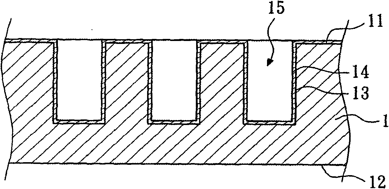
Figure 1 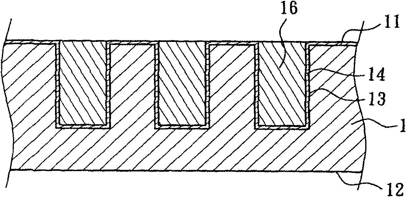
Figure 2 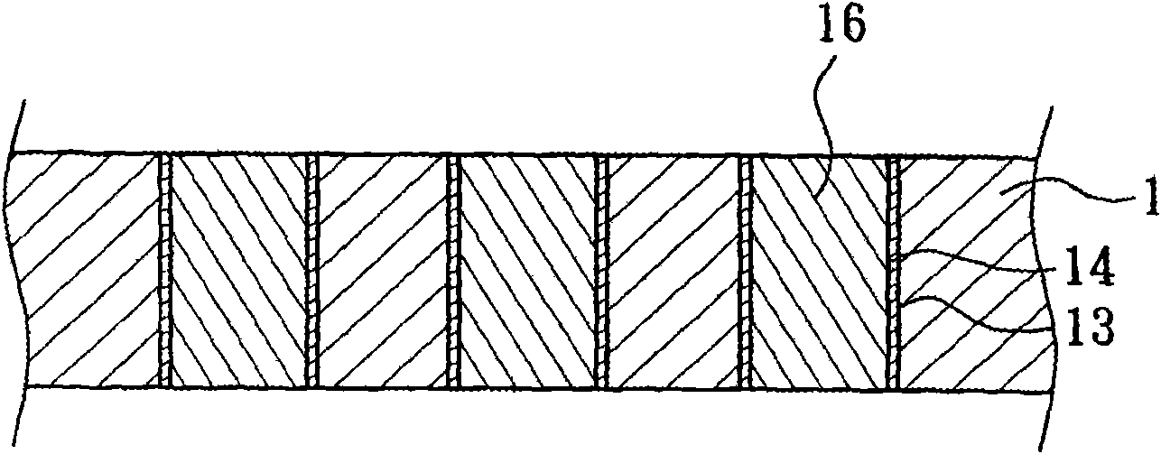
Figure 3
Abstract
Description
Technical field
[0001] The present invention relates to a method for forming a through hole on a substrate and a substrate with a through hole. In detail, it relates to a method for forming an insulating layer on the sidewall of a through hole using a polymer and A substrate with the through hole. Background technique
[0002] Referring to FIGS. 1 to 3, a schematic diagram of a known method of forming a via hole on a substrate is shown. First, referring to FIG. 1, a substrate 1 is provided. The substrate 1 has a first surface 11 and a second surface 12. Next, a number of grooves 13 are formed on the first surface 11 of the substrate 1. Then, an insulating layer 14 is formed on the sidewalls of the trenches 13 by using a chemical vapor deposition (CVD) method, and a plurality of accommodating spaces 15 are formed. The material of the insulating layer 14 is usually silicon dioxide.
[0003] Next, referring to FIG. 2, a conductive metal 16 is filled in the accommodating spaces 15....
Examples
Embodiment Construction
[0105] reference Figure 4 to Figure 21 , Showing a schematic diagram of the first embodiment of the method for forming via holes on a substrate of the present invention. First, refer to Figure 4 and Figure 5 ,among them Figure 4 Is the top view of the substrate, Figure 5 for Figure 4 Section along line 5-5 in the middle. A substrate 21 is provided, and the substrate 21 has a first surface 211 and a second surface 212. The substrate 21 can be a silicon substrate or a wafer. Next, a slot 231 is formed on the first surface 211 of the substrate 21. The slot 231 has a side wall 232 and a bottom surface 233. In this embodiment, a first photoresist layer 241 is formed on the substrate 21. The first surface 211 is formed on the first photoresist layer 241 with a first opening 242.
[0106] Next, refer to Image 6 According to the first opening 242, a groove 231 is formed on the substrate 21 by etching. The slot 231 is located on the first surface 211 of the substrate 21 and has a...