
Wire connecting method for line repair
A wiring and circuit technology, applied in the field of semiconductor circuit repair, can solve problems such as accidental short circuit, poor contact, platinum discontinuity, etc., and achieve the effect of improving current function debugging, improving success rate and saving costs.
Patent Information
- Authority / Receiving Office
- CN · China
- Patent Type
- Applications(China)
- Current Assignee / Owner
- Publication Date
- 2011-05-25
Smart Images
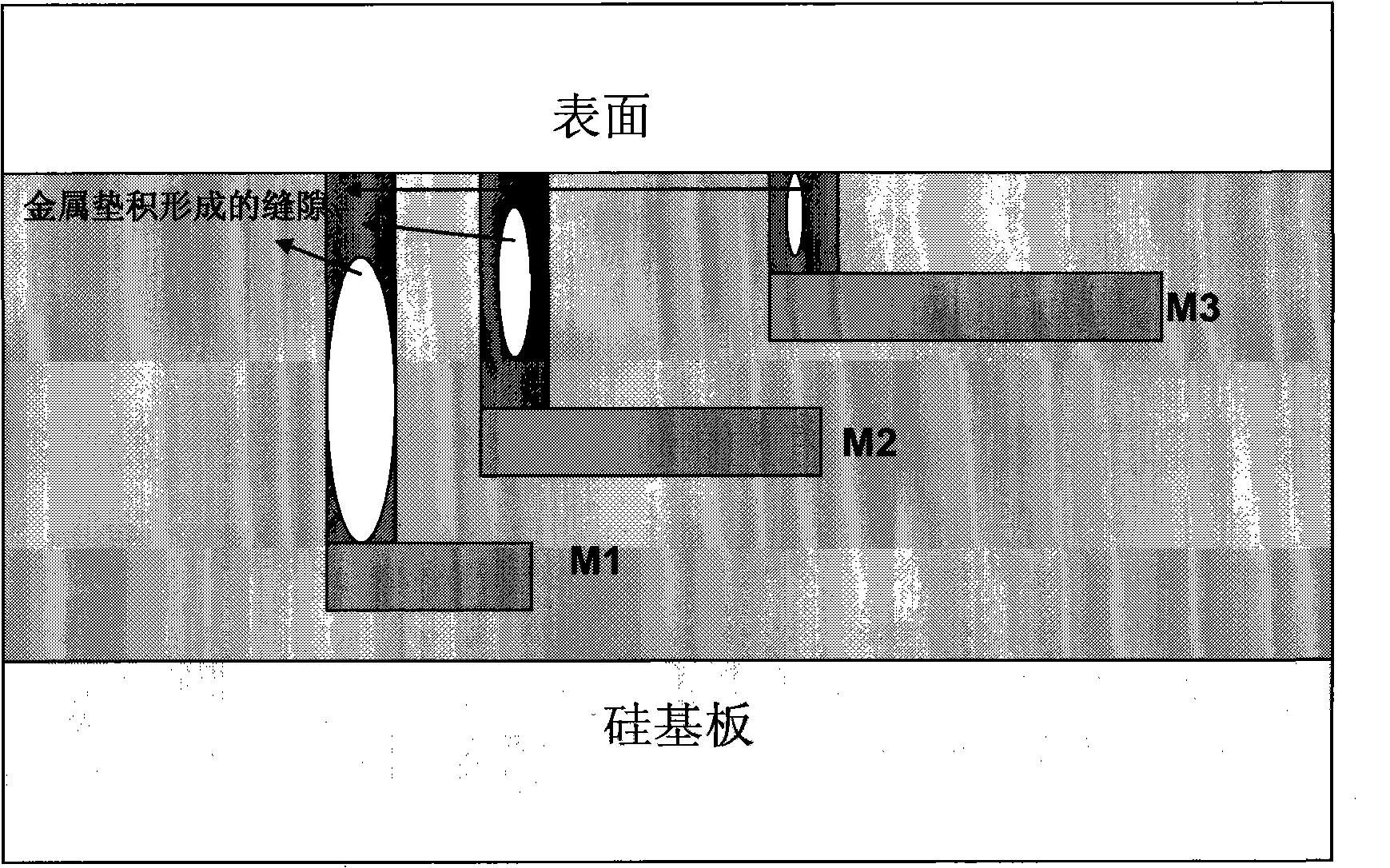
Figure 1 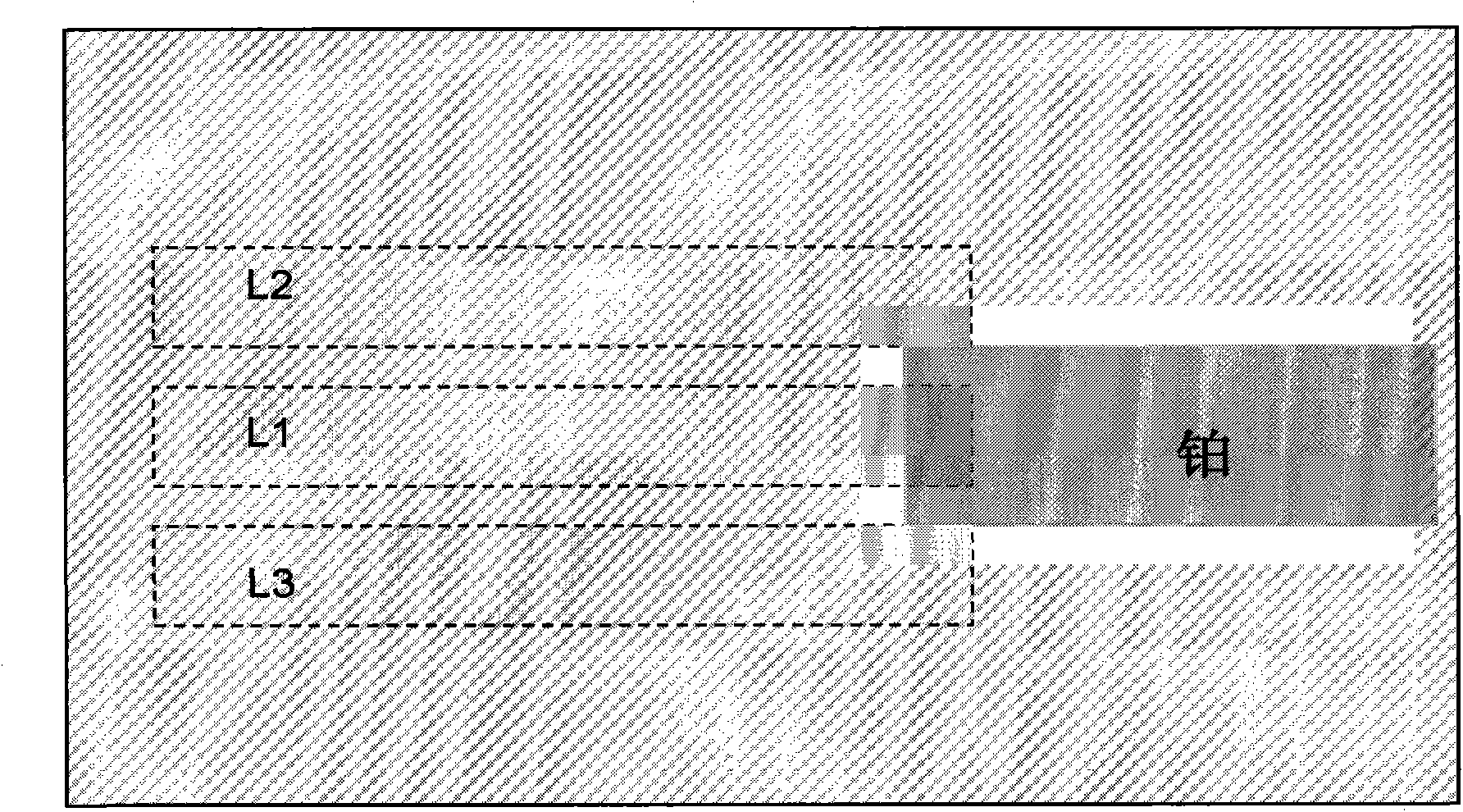
Figure 2 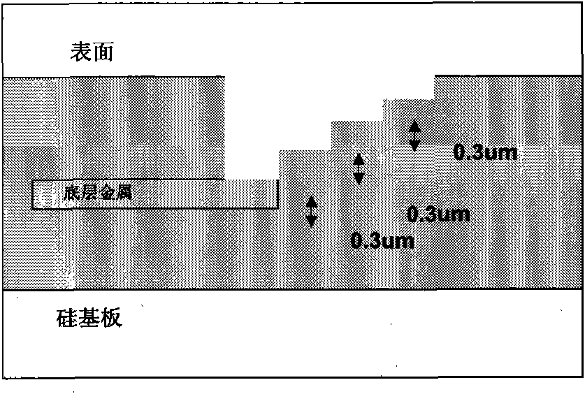
Figure 3
Abstract
Description
technical field
[0001] The invention relates to a semiconductor circuit repair method, in particular to a circuit repair technology used in semiconductor chip debugging and failure analysis. Background technique
[0002] At present, the direct etching single window connection method of the focused particle beam electron microscope FIB (Focused Ion Beam) commonly used in the field of semiconductor circuit repair has the following problems:
[0003] 1. When the metal line to be repaired is more than 2 layers of metal layer and insulating layer (or more than 1 micron in height) from the surface of the silicon chip, due to the large drop, when the platinum is plated, there will be poor contact, resulting in a large impedance Or not connected at all, the performance is (1) When the window is small, the platinum deposition process is similar to the metal sputtering filling in the semiconductor process. The larger the aspect ratio, the larger the gap in the middle of the hole, resu...
Examples
Embodiment Construction
[0028] Focused Ion Beam Electron Microscope FIB (Focused Ion Beam): It uses the focused gallium positive ion beam as the incident particle (or primary ion) to hit the surface of the sample, and collects secondary electrons for imaging. Due to the large atomic weight of gallium ions, it accelerates The rear kinetic energy is large, so it has a good sputtering etching function, and with a suitable gas system, auxiliary functions including selective etching and depositing specific materials can be realized. The gas system it is often equipped with is Pt-Dep (platinum metal deposition system), IEE (selective enhanced etching), I-dep (insulation film deposition), etc.; when working, the gas is sprayed on the surface of the sample, and the ion beam bombards When FIB sets the pattern, it not only directly etches the sample surface, but also impacts some gas atoms on the sample surface; by adjusting appropriate parameters, a layer of platinum metal film can be deposited with Pt-dep, an...