
Chaotic circuit applicable to AD (analog-to-digital) conversion and random binary sequence generation
A binary sequence, chaotic circuit technology, applied in the chaotic field, can solve the problems of non-uniform bias output voltage, high circuit cost, high power consumption, etc., and achieve the effects of high conversion accuracy, simple circuit and strong adaptability
Patent Information
- Authority / Receiving Office
- CN · China
- Patent Type
- Applications(China)
- Current Assignee / Owner
- Publication Date
- 2013-09-18
Smart Images
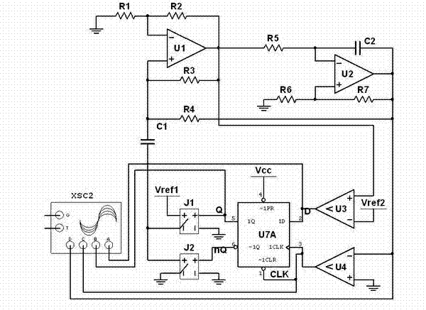
Figure 1 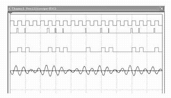
Figure 2 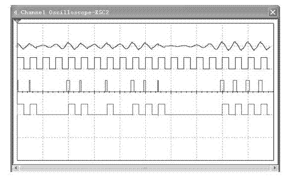
Figure 3
Abstract
Description
technical field
[0001] The invention relates to the technical field of chaos. In particular, it relates to a chaotic circuit suitable for AD conversion and generating random binary sequences. Background technique
[0002] One of the most important properties of chaotic systems is initial value sensitivity. Initial value sensitivity indicates that a nonlinear system has a high resolution to the initial value in the chaotic state. This characteristic can be used in small-signal measurement in nature, parameter estimation and A / D conversion technology, etc.
[0003] An analog-to-digital converter, namely ADC, as a device that converts a continuous signal in analog form to a discrete signal in digital form, is widely used in communication, computer, control and detection and other fields. The accuracy of traditional ADCs is easily affected by device nonlinearities. Using the chaotic initial value sensitivity to design ADC can eliminate the influence of component parasitic pa...
Examples
Embodiment 1
[0039] Implementation 1: The chaotic oscillator of the present invention is used as a true random sequence generator. The specific steps include:
[0040] Figure (2) is the implementation circuit of the chaotic circuit as a true random sequence generator, assuming that the current flowing through R3 is , the current flowing through R4 is , the current flowing through capacitor C1 is , the current flowing through resistor R5 is , the output of U1 is the voltage , the output voltage of U2 is . According to the principle of virtual short and virtual break of the ideal operational amplifier, the voltage on the capacitor C1 can be deduced as , the voltage on capacitor C2 for , and according to Kirchhoff’s voltage and current law KVL and KCL, the relationship between the variables is as follows:
[0041]
[0042] From the above relationship, it can be deduced that:
[0043]
[0044] So far, according to the parameter relationship and state equation given in t...
Embodiment 2
[0049] Implementation 2: The specific steps of using the chaotic oscillator of the present invention as an analog-to-digital converter (ADC) include:
[0050] When the circuit is applied as an analog-to-digital converter (ADC), an input sampling circuit can be added to sample the input analog waveform to C1. During theoretical simulation, since the circuit in the present invention can generate an internal clock signal, the method of assigning an initial value to the capacitor C1 can be used. However, in practical applications, corresponding circuit modules need to be designed to realize it. We give an example of building a sample and hold circuit module in Implementation 2, indicating that if the chaotic circuit is used as an A / D converter, a sample and hold module for analog signals should be added. As shown in Figure (4), IO1 is the analog signal input module of the sampling and holding part, U5 is an operational amplifier, and the capacitors C1 and C2 are controlled by com...