
A Large Numerical Aperture Immersion Projection Objective
A technology of projection objective lens and numerical aperture, which is applied in the field of projection optics, can solve problems such as material type limitations, achieve good imaging characteristics, improve lithography resolution, and reduce the difficulty of assembly and integration
Patent Information
- Authority / Receiving Office
- CN · China
- Patent Type
- Patents(China)
- Current Assignee / Owner
- Publication Date
- 2016-09-28
- Estimated Expiration
- Not applicable · inactive patent
Smart Images
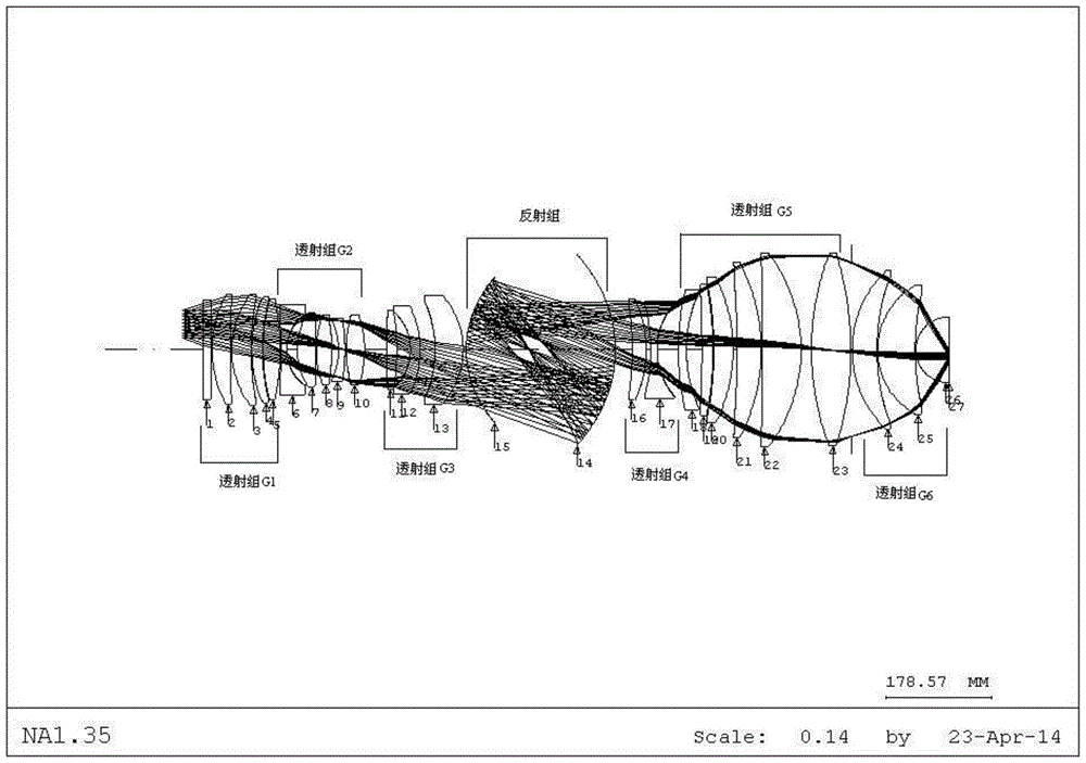
Figure 1
Abstract
Description
technical field
[0001] The invention relates to a large numerical aperture immersion type projection objective lens used in lithography technology and semiconductor element manufacturing device, which belongs to the technical field of projection optics. Background technique
[0002] Lithography is an integrated circuit manufacturing technology. It uses the principle of optical projection image to transfer the high-resolution graphics on the mask plate to the optical exposure process of the rubber-coated silicon wafer by means of exposure. Almost all integrated circuits Fabrication is done using optical projection lithography.
[0003] With the continuous advancement of science and technology, various types of semiconductor chips are widely used in aerospace, military, and civilian fields such as computers. With the continuous improvement of equipment performance requirements, the resolution requirements for semiconductor chips are getting higher and higher. At present, the ...
Examples
Embodiment Construction
[0033] In order to better illustrate the purpose and advantages of the present invention, the present invention will be further described below in conjunction with the accompanying drawings and specific embodiments.
[0034] figure 1 It is a schematic diagram of the layout of the large numerical aperture immersion projection objective lens of the present invention. 26 optical elements form the transmission group G1, the transmission group G2, the transmission group G3, the reflection group, the transmission group G4, the transmission group G5, and the transmission group G6, sequentially from the beam incident direction set up.
[0035] The transmission group G1 is a unit group with a positive focal length, including the first positive lens 1, the second positive lens 2, the third positive lens 3, the fourth positive lens 4, and the first negative lens 5. The light is projected from the object plane through the transmission group After G1 converges, it enters the transmission ...