
A Thin Film Transistor with Improved Drain Current
A thin-film transistor and drain current technology, applied in the direction of transistors, circuits, electrical components, etc., can solve problems such as jumping difficulties, carrier mobility decline, carrier occupation density of states, etc.
Patent Information
- Authority / Receiving Office
- CN · China
- Patent Type
- Patents(China)
- Current Assignee / Owner
- Publication Date
- 2017-11-17
Smart Images
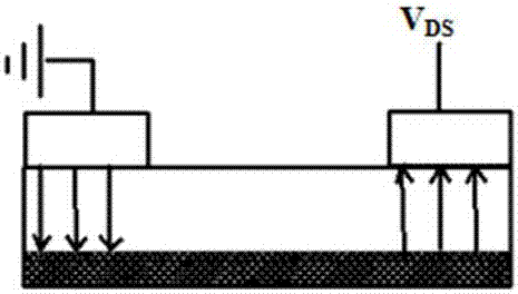
Figure 1 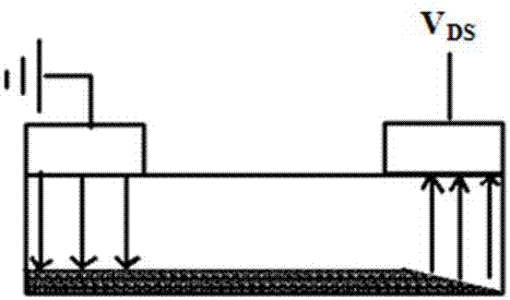
Figure 2 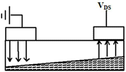
Figure 3
Abstract
Description
technical field
[0001] The invention relates to the technical field of thin film transistor preparation, in particular to a thin film transistor preparation method for improving drain current. Background technique
[0002] As a core component in active driving, a thin film transistor includes several important components such as a substrate, a semiconductor channel layer, a dielectric layer, a gate, a source, and a drain. Thin film transistors are used as switching elements, that is, they only work in the two extreme conditions of on state (on) and off state (off). The switching current ratio is an important parameter of the device, which represents the sensitivity of the element, that is, the switching speed. High means that the switching speed of the component is faster, and the display effect can be better controlled. Therefore, in order to obtain a higher switching current ratio, the on-state current (also called the drain current) can be increased. The on-state curren...
Examples
Embodiment 1
[0040] N-type doping is carried out on the semiconductor layer, and the preparation scheme of each structural layer is as follows:
[0041] (1) A layer of 104 zinc oxide (ZnO) is sputtered on the 102 insulating layer film by sputtering process, and the thickness is controlled at 50-300nm;
[0042] (2) Indium is implanted into the active layer 104 by means of ion implantation. By controlling the energy and dose, the doped layer 103 presents a gradient shape. The implanted energy is set at 50-100kV, and the indium is doped according to the energy In a gradient shape, the dose is controlled at 1×10 16 / cm 2 ;
[0043] (3) The doped device is annealed in air, and the annealing temperature is 980°C;
[0044] (4) Depositing an aluminum film on the active layer 104 by vacuum evaporation technology;
[0045] (5) Use a spin coater to spin coat a layer of photoresist on the aluminum film, and then bake and cure;
[0046] (6) Use a specific mask to expose it to ultraviolet rays;
...
Embodiment 2
[0052] P-type doping is performed on the semiconductor layer, the substrate is Si, and the insulating layer is SiO 2 , the source and drain electrodes are Al, the preparation scheme of each structure is similar to that of Example 1, and the doping material is replaced by P 2 o 5 , ionized with an ion implanter and then doped with phosphorus.