
Wave trough breakover control circuit and control method thereof
A conduction control circuit, wave trough technology, applied in the direction of electrical components, high-efficiency power electronic conversion, output power conversion devices, etc., can solve the problems of not improving efficiency, limited input voltage, etc., to achieve jitter and improve electromagnetic interference , The effect of improving energy efficiency
Patent Information
- Authority / Receiving Office
- CN · China
- Patent Type
- Applications(China)
- Current Assignee / Owner
- Publication Date
- 2016-05-11
Smart Images
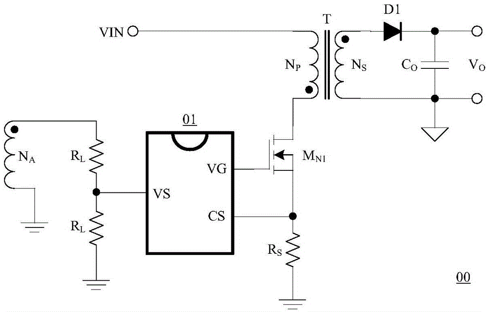
Figure 1 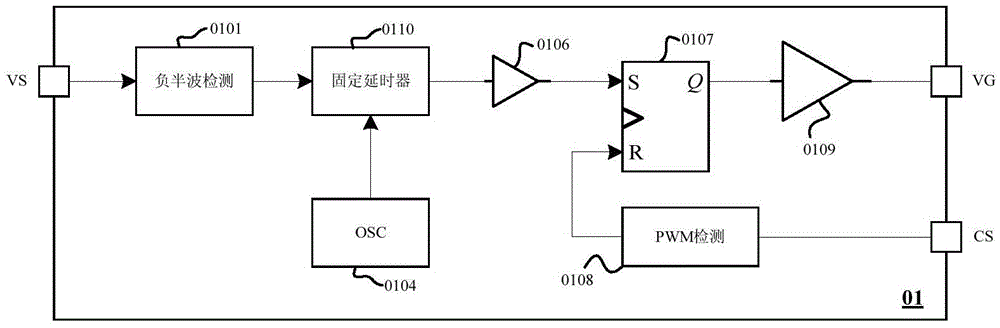
Figure 2 
Figure 3
Abstract
Description
technical field
[0001] The invention relates to a switching power supply, in particular to a valley conduction control circuit and a control method thereof for controlling a switch tube to be turned on and turned off at a proper time. Background technique
[0002] With the rapid development of science and technology, the application of consumer electronics is becoming more and more popular, and the integration of transistors is advancing according to Moore's Law. The number of devices contained in the same wafer area is increasing, and the size of devices is also increasing. This not only leads to higher and higher requirements for energy, but also leads to the fact that the power supply voltage used by integrated circuits has become lower, and the driving ability of the signal will become weaker, which has also led to the chip's ability to resist electromagnetic interference. Ability requirements have become more stringent. In the current ACDC switching power supply indust...
Examples
Embodiment 1
[0043] figure 1 It is a schematic block diagram of a flyback ACDC topology switching power supply. The switching power supply 00 system includes a transformer T, and the transformer T has a primary winding N P , secondary winding N S and auxiliary winding N A , used to transfer energy and signal feedback; power supply input terminal VIN, primary side ground, control system 01, first resistor R H , the second resistance R L , the first N-type MOS tube MN1, the third resistor sampling resistor R S , the first diode D1, the first capacitor Co, the positive output voltage terminal of the secondary side, and the ground of the secondary side. The first terminal of the primary winding NP, the second terminal of the secondary winding NS and the first terminal of the auxiliary winding NA of the transformer T are terminals with the same name. Description of primary side connection relationship: primary side winding N P The first end of the transformer T is connected to the power ...