
Process method for improving interlayer alignment accuracy in multilayer co-fired ceramic circuit processing
A technology for circuit processing and alignment accuracy, which is applied in multi-layer circuit manufacturing, printed circuit, circuit substrate materials, etc., which can solve the problem of ensuring precise control of thickness uniformity, decreased interlayer alignment accuracy, and lack of wide applicability, etc. problem, to achieve the effect of versatility, increased interlayer stability, and good dimensional stability
Patent Information
- Authority / Receiving Office
- CN · China
- Patent Type
- Applications(China)
- Current Assignee / Owner
- Publication Date
- 2017-08-15
Smart Images
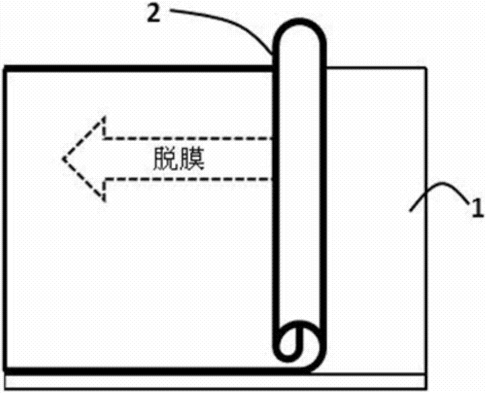
Figure 1 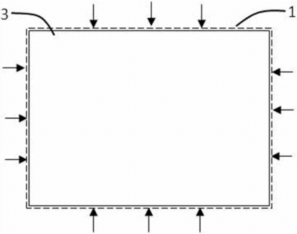
Figure 2 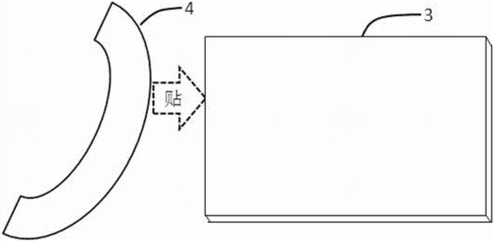
Figure 3
Abstract
Description
technical field
[0001] The invention belongs to the field of multilayer co-fired ceramic circuit processing, and specifically relates to a process method for improving interlayer alignment accuracy in multilayer co-fired ceramic circuit processing. Alignment accuracy. Background technique
[0002] The multi-layer co-fired ceramic circuit represented by LTCC (low temperature co-fired ceramic) has outstanding advantages such as high integration density, microwave / digital / control multi-functional hybrid integration, excellent high-frequency performance, etc., and has gradually become a miniaturized, high-performance T It is the first choice to implement circuit substrates such as / R components, frequency sources, and phased array antennas, and has been widely used in aviation, aerospace, missile-borne, ship-borne and other fields.
[0003] The conventional production process of multi-layer co-fired ceramic circuit boards is: raw porcelain cutting→green porcelain drilling→green...
Examples
Embodiment 1
[0046] 1) After the raw porcelain is cut into the standard process size, tear off the Mylar film 2 that comes with the raw porcelain from the green porcelain 1, as shown in figure 1 shown.
[0047] 2) Dry the green porcelain 1 without film at 60°C for 30 minutes to obtain green porcelain 3 with proper deformation, such as figure 2 shown.
[0048] 3) Paste the organic film 4 coated with a 1 μm low-viscosity coating on one side on the deformed green porcelain 3, as shown in image 3 shown. The thickness of the organic membrane 4 is 50 μm.
[0049] 4) The raw porcelain after the second film is like Figure 4 As shown, the green ceramic 3 and the organic film 4 are well bonded, and the green ceramic can maintain a low amount of deformation during the process of multilayer co-fired ceramic circuits.
[0050] 5) The processing is completed by conventional multi-layer ceramic circuit processes such as punching, filling, printing, stripping, and lamination.
Embodiment 2
[0052] 1) After the raw porcelain is cut into the standard process size, tear off the Mylar film 2 that comes with the raw porcelain from the green porcelain 1, as shown in figure 1 shown.
[0053] 2) The green porcelain 1 without film is placed naturally in a 100,000-class purification environment for 8 hours to obtain green porcelain 3 with proper deformation, such as figure 2 shown.
[0054] 3) Paste the organic diaphragm 4 coated with a 2.5 μm low-viscosity coating on one side on the deformed raw porcelain 3, as shown in image 3 shown. The thickness of the organic membrane 4 is 75 μm.
[0055] 4) The raw porcelain after the second film is like Figure 4 As shown, the green ceramic 3 and the organic film 4 are well bonded, and the green ceramic can maintain a low amount of deformation during the process of multilayer co-fired ceramic circuits.
[0056] 5) The conventional multilayer ceramic circuit technology of punching, hole filling, printing, stripping, lamination...
Embodiment 3
[0066] 1) Tear off the Mylar film A-2 of the original green porcelain A from the green porcelain A-1, and then stick the organic film B coated with the adhesive coating B-1 on a hot stage at 40°C On the back of the green porcelain, the bonding coating is in contact with the back of the green porcelain to form a new structure C. see Figure 5-7 .
[0067] 2) Fabricate through holes 1-1, conductor patterns 1-2, and cavities 1-3 in the first layer of the product on structure C using conventional processes. J-1 is a through hole for optical alignment, and J-2 is an alignment hole for pin stacking, such as Figure 8 shown.
[0068] 3) According to the method in 2), the processing of each layer of raw porcelain except the last layer is completed on the new structure C, such as Figure 9-10 shown.
[0069] 4) Use the conventional process to complete the through hole L-1, the conductor pattern L-2, the through hole J-1 for optical alignment, and the alignment hole J-2 for pin lam...