

Encapsulation structure and method of micro electro mechanical system device
A micro-electro-mechanical system and packaging structure technology, which is applied in the direction of micro-electronic micro-structure devices, micro-structure technology, electric solid-state devices, etc., can solve the problems of high process difficulty, high cost, and low air-tightness, and achieve simple manufacturing process and high production efficiency. Low cost and good air tightness
Patent Information
- Authority / Receiving Office
- CN · China
- Patent Type
- Applications(China)
- Current Assignee / Owner
- Publication Date
- 2017-08-18
- Estimated Expiration
- Not applicable · inactive patent
Smart Images
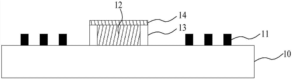
Figure 1 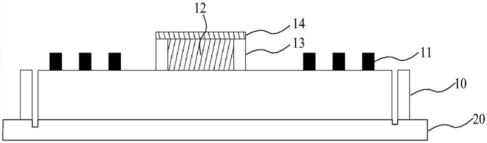
Figure 2 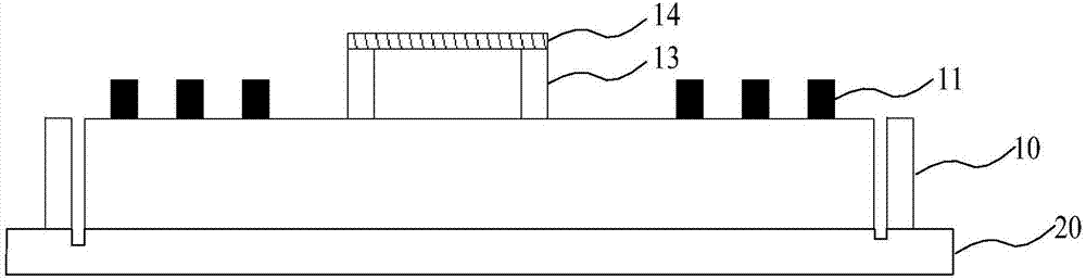
Figure 3
Abstract
Description
technical field
[0001] The invention relates to the technical field of semiconductor packaging, in particular to a packaging structure and method for micro-electromechanical system devices. Background technique
[0002] Micro-Electro-Mechanical System (MEMS) sensor is a new type of sensor manufactured by microelectronics and micromachining technology. Compared with traditional sensors, it has the characteristics of small size, light weight, low cost, low power consumption, high reliability, suitable for mass production, easy integration and intelligentization.
[0003] Since most MEMS devices have airtightness requirements, such as a microbolometer (Micro-bolometer) in the infrared sensor, in the prior art, the packaging method of the MEMS sensor usually adopts a cap that forms a closed space, Through-silicon vias are formed on the cap to realize the electrical connection of MEMS and meet airtightness requirements, but the traditional packaging method requires additional pr...
Examples
Embodiment Construction
[0037] Such as Figure 1 to Figure 4 As shown, it is a structural diagram corresponding to each step in an infrared sensor packaging method well known to the inventor. First, if figure 1 As shown, a first substrate 10 is provided, which includes a corresponding circuit structure, and then a number of contact holes 11 are formed on the first plane of the first substrate 10 for realizing the circuit structure. External electrical connection; In addition, a sacrificial layer 12 is formed on the first plane of the first substrate 10, and the sacrificial layer 12 can be commonly used materials such as silicon oxide, amorphous silicon or photosensitive polyimide; A microbridge structure 13 is formed on the sidewall of the sacrificial layer 12, and a photosensitive material layer 14 is formed, and the photosensitive material layer covers the sacrificial layer 12 and the microbridge structure 13. The above structures can be collectively referred to as a chip to be packaged. circle; ...