
Lateral high-voltage device
A lateral high voltage, device technology, applied in semiconductor devices, electrical components, circuits, etc., can solve problems such as larger than on-resistance, and achieve the effect of reducing on-resistance, reducing device surface area, and reducing device area
Patent Information
- Authority / Receiving Office
- CN · China
- Patent Type
- Applications(China)
- Current Assignee / Owner
- Publication Date
- 2017-10-20
Smart Images
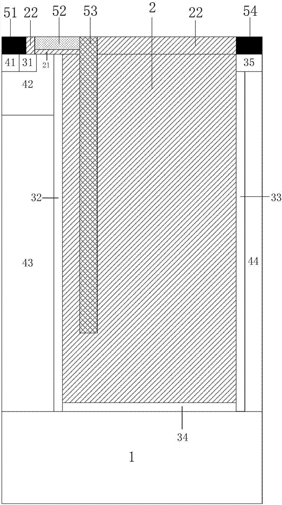
Figure 1 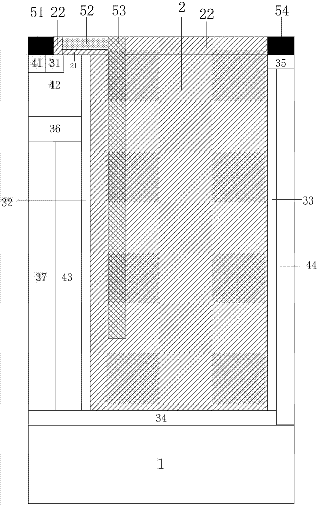
Figure 2 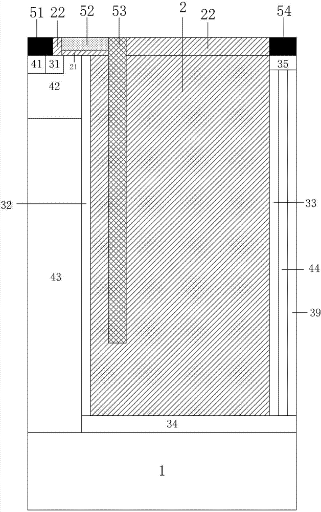
Figure 3
Abstract
Description
technical field
[0001] The invention belongs to the technical field of semiconductor power devices, and in particular relates to a lateral high voltage device. Background technique
[0002] Lateral Double-diffused Metal-Oxide-Semiconductor Field Effect Transistor (LDMOSFET), as the core device in Power Integrated Circuit (PIC), has the advantages of easy integration and low driving power. , negative temperature coefficient and other advantages, it has been developing in the direction of high breakdown voltage (Breakdown Voltage, BV) and low specific on-resistance (Specific On-Resistance, Ron, sp) for many years. A higher breakdown voltage requires a device with a longer drift region length and a lower drift region doping concentration, which results in a device with a higher on-resistance. This contradictory relationship between breakdown voltage and specific on-resistance is the "silicon limit" problem that plagues the industry.
[0003] In order to alleviate this contrad...
Examples
Embodiment 1
[0039] like figure 2As shown, a lateral high-voltage device includes: a dielectric groove 2, and the left side of the dielectric groove 2 is provided with doped stripe overlapping structures alternately arranged with different doping types, and the doped stripe overlapping structure sequentially includes the first N-type doped The strip 32 , the first P-type doped strip 43 , the fifth N-type doped strip 37 , and the fourth N-type doped strip 36 is located between the doped-strip overlapping structure and the P-well region 42 . The upper surface of the dielectric groove 2 is a dielectric layer 22, and the body field plate 53 extends from the upper surface of the device to the inside of the dielectric groove 2. The body field plate 53 is adjacent to the polysilicon gate 52, and the underside of the polysilicon gate 52 is the under-gate oxide layer 21, the source The contact electrode 51 and the polysilicon gate 52 are separated by the dielectric layer 22, the body field plate 5...
Embodiment 2
[0045] like image 3 As shown, the present invention is basically the same as the embodiment 1, the difference is that the overlapping structure of doped strips is located on the right side of the dielectric groove 2 . When the doped strip overlapping structure is on the right side of the dielectric groove 2, the doped strip overlapping structure sequentially includes a second N-type doped strip 33, a second P-type doped strip 44, and a seventh N-type doped strip 39, and The top surfaces of the N-type doped strips 33 , P-type doped strips 44 and N-type doped strips 39 are in contact with the second N-type heavily doped region 35 .
Embodiment 3
[0047] like Figure 4 As shown, the present invention is basically the same as the embodiment 1, the difference is that: the overlapping structure of doped strips is located under the dielectric groove 2 . When the doped-strip overlapping structure is below the dielectric trench 2 , the doped-strip overlapping structure sequentially includes a third N-type doped strip 34 , a third P-type doped strip 45 , and a sixth N-type doped strip 38 .