
A slotted gate power device with enhanced anti-single event capability
A power device, anti-single particle technology, applied in electric solid state devices, semiconductor/solid state device components, semiconductor devices, etc., can solve the problems of large application limitations, suppressing parasitic transistors, difficult process implementation, etc., to reduce holes Current, Enhanced Reliability, Effect of Enhanced Reliability
Patent Information
- Authority / Receiving Office
- CN · China
- Patent Type
- Patents(China)
- Current Assignee / Owner
- Publication Date
- 2020-07-17
Smart Images
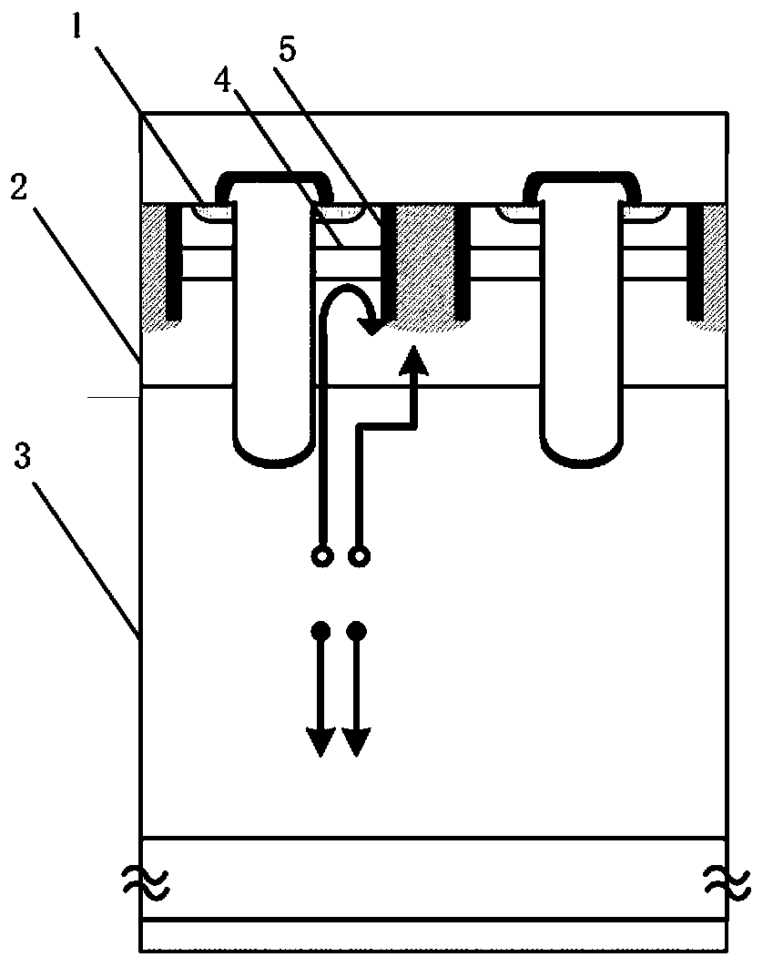
Figure 1
Abstract
Description
technical field
[0001] The present application relates to the field of semiconductor devices, in particular to a slot-type gate power device reinforced with enhanced anti-single event capability. Background technique
[0002] Trench power MOSFETs with trench gate structure are widely used in the field of power control due to their advantages of low on-state voltage drop, high frequency operation capability, simple drive control, and easy parallel connection. However, in harsh environments, the device's anti-single event ability is poor.
[0003] However, in the process of realizing the application technical solution in the embodiment of the application, the applicant of the present application found that the above-mentioned technology has at least the following technical problems:
[0004] The methods for improving the anti-single particle capability in the prior art have the technical problems of relatively large application limitations and difficult process implementation...
Examples
Embodiment 1
[0019] The embodiments of the present application provide a grooved gate power device with enhanced anti-single event capability, and the power field effect transistor is also called PowerMOS field effect transistor. In practical applications, it has better power handling characteristics than bipolar transistors and CMOS field effect transistors. Such as figure 1 shown, the transistors include:
[0020] The N+ source contact 1, the Pwell region 2, the N drift region 3 and the deep groove polysilicon gate form a gate-controlled field-effect transistor structure; the N-type hole blocking layer 4 can block the flow of holes to the N+ region, and the Pwell region Both sides of the deep groove structure are filled with thick oxide layer dielectric 5, and a P+ region is formed at the bottom of the deep groove structure in the Pwell region to absorb hole carriers.
[0021] Specifically, two PN junctions are formed between two differently doped P regions and a layer of lowly doped N...
Embodiment 2
[0029] In order to more clearly describe a slotted gate power device with enhanced anti-single event capability, the embodiment of the present application also provides a working principle of a slotted gate power device with enhanced anti-single event capability. The following is a The working principle of the reinforced groove gate power device with enhanced anti-single event capability is described in detail.
[0030] The structure of this application adds an N-type hole blocking layer 4 under the N+ source 1 to block the flow of holes; at the same time, the source contact adopts grooves to pass through the N-type hole blocking layer 4 area, providing a hole The collection channel flowing to the source, the two sides of the groove structure are thick oxide layer 5 sidewalls, the hole blocking layer 4 is not in contact with the source and has an electrical connection, it only serves as a hole blocking effect, avoiding the N-type hole blocking layer 4 is electrically connected...