
Preparation method of driving substrate
A technology for driving substrates and driving areas, which is applied in semiconductor/solid-state device manufacturing, semiconductor/solid-state device components, diodes, etc., and can solve problems such as uneven display on the screen
Patent Information
- Authority / Receiving Office
- CN · China
- Patent Type
- Patents(China)
- Current Assignee / Owner
- Publication Date
- 2020-01-10
Smart Images
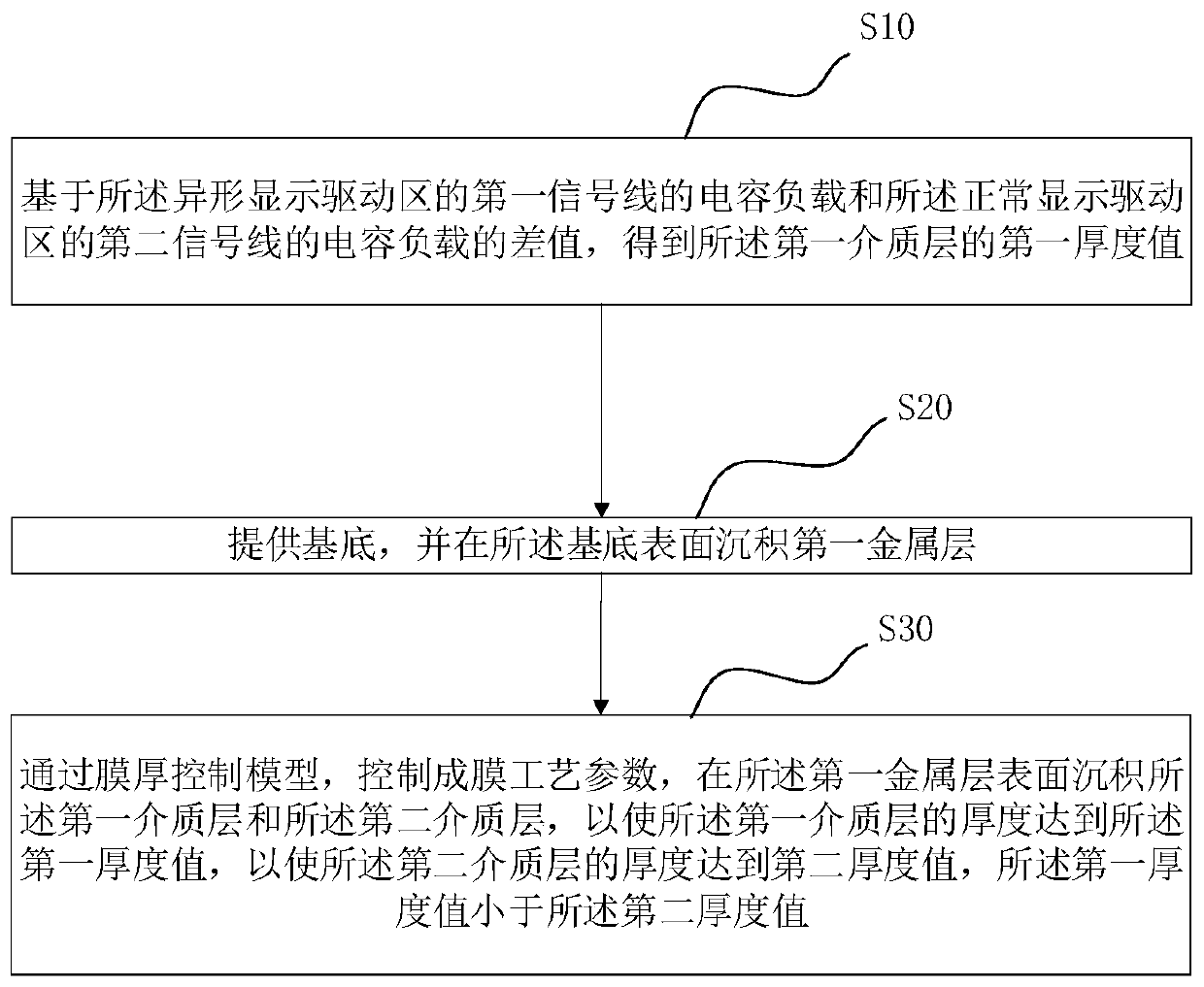
Figure 1 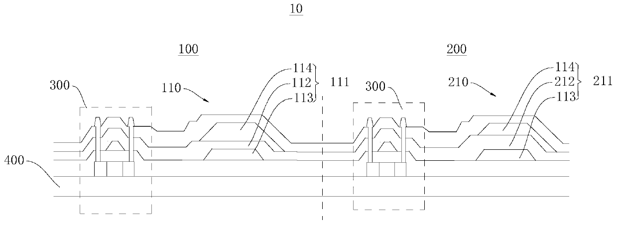
Figure 2 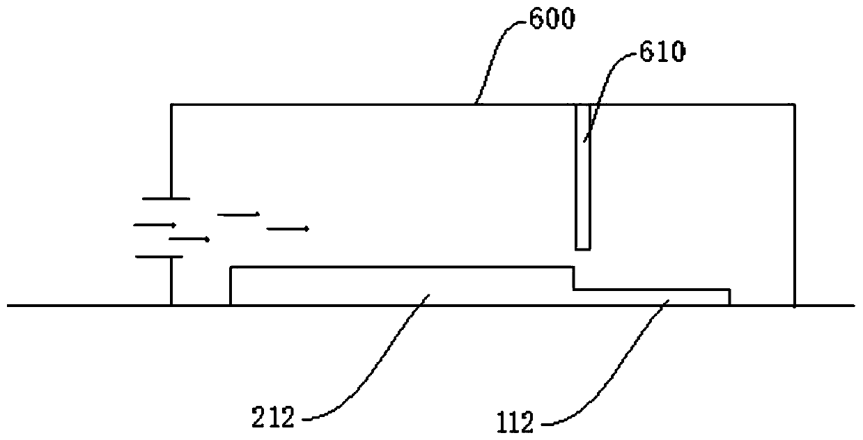
Figure 3
Abstract
Description
technical field
[0001] The present application relates to the display field, in particular to a method for preparing a driving substrate. Background technique
[0002] With the continuous development of the mobile phone industry, the screen body of a full-screen mobile phone has the advantages of a large screen-to-body ratio and a narrow frame, which greatly improves the visual effect of the viewer and has attracted widespread attention.
[0003] In the production process of the full screen, the special-shaped display area is usually formed by special-shaped designs such as slots on the screen body. The number of pixels at the slot is less than the number of pixels in the normal display area. Therefore, the load of the pixel driving signal in the special-shaped display area is very different from that of the normal display area, resulting in different RC delays of driving signals such as pixel scanning, resulting in different brightness between the special-shaped display ar...
Examples
Embodiment Construction
[0048] In order to facilitate the understanding of the present invention, the present invention will be described more fully below with reference to the associated drawings. Preferred embodiments of the invention are shown in the accompanying drawings. However, the present invention can be embodied in many different forms and is not limited to the embodiments described herein. On the contrary, these embodiments are provided to make the understanding of the disclosure of the present invention more thorough and comprehensive.
[0049] See figure 1 and figure 2 , the embodiment of the present application provides a method for manufacturing a driving substrate. The driving substrate 10 includes a substrate 400 , and a special-shaped display driving region 100 and a normal display driving region 200 disposed adjacently between surfaces of the substrate 400 . The special-shaped display driving region 100 includes a plurality of first driving circuit units 110 arranged at interv...