
Semiconductor laser bar and semiconductor outer cavity
A semiconductor and laser technology, used in semiconductor lasers, optical waveguide semiconductor structures, lasers, etc., can solve the problems of periodic field deterioration, high precision requirements, and difficult implementation.
Patent Information
- Authority / Receiving Office
- CN · China
- Patent Type
- Applications(China)
- Current Assignee / Owner
- Publication Date
- 2021-04-20
- Estimated Expiration
- Not applicable · inactive patent
Smart Images
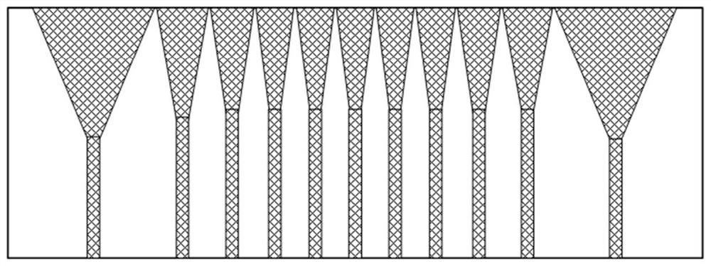
Figure 1 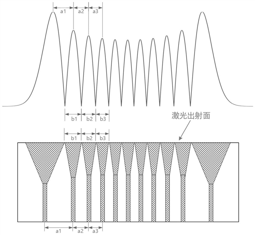
Figure 2 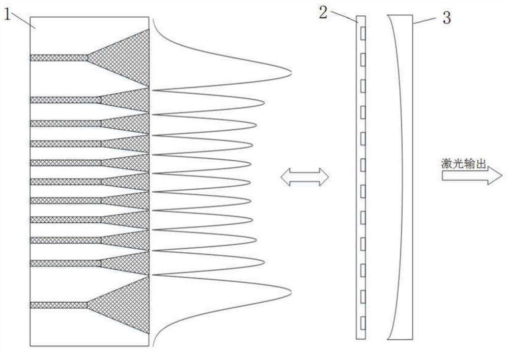
Figure 3
Abstract
Description
technical field
[0001] The invention belongs to the field of coherent beam combining of semiconductor laser arrays, and more specifically relates to a semiconductor laser bar and a semiconductor external cavity. Background technique
[0002] Semiconductor laser has always been the frontier hotspot of laser research. The biggest problem limiting the wide application of high-power semiconductor lasers is their poor beam quality. At present, the spectral beam combining technology is mainly used to improve the brightness of high-power semiconductor lasers. This method greatly improves the brightness of the semiconductor laser array. However, in the process of advancing the semiconductor laser to a higher power, it is limited by the semiconductor gain bandwidth and cannot achieve a larger number of semiconductor laser beams. In addition, spectral beam combining technology usually requires a relatively complex coating technology as the basis, which is difficult to realize. [0...
Examples
Embodiment 1
[0034] figure 1 A schematic structural diagram of a semiconductor laser bar provided by an embodiment of the present invention. refer to figure 1 , combined with figure 2 , the structure of the semiconductor laser bar in this embodiment will be described in detail.
[0035] The semiconductor laser bar includes a plurality of light-emitting units and non-light-emitting areas between adjacent light-emitting units. refer to figure 2, the light-emitting unit corresponds to the peak of the high-order Hermitian-Gaussian beam one-to-one, the non-luminous area corresponds to the nodal line of the high-order Hermitian-Gaussian beam, and the width of each light-emitting unit is equal to the width between the zero points at both ends of the corresponding wave peak , each non-light-emitting area coincides with its corresponding node line, and the width of each light-emitting unit is not equal. Among them, the high-order Hermitian Gaussian beam is generated by the interaction between...
Embodiment 2
[0039] image 3 It is a schematic structural diagram of the semiconductor external cavity provided by the first embodiment of the present invention. refer to image 3 , combined with Figure 4A with Figure 4B , the structure of the semiconductor external cavity in this embodiment will be described in detail.
[0040] refer to image 3 , the semiconductor external cavity includes a semiconductor laser bar 1 , a diffractive optical element 2 and an output mirror 3 distributed in sequence. Semiconductor laser bar 1 is such as Figure 1-Figure 2 Semiconductor laser bar in the illustrated embodiment. The diffractive optical element 2 is used to control the intracavity mode to realize high-order Hermitian mode oscillation to generate a high-order Hermitian Gaussian beam. The output mirror 3 is used to couple out the high-order Hermitian Gaussian beam, provide part of the coupled output, and feed back another part of the laser light back into the cavity for further amplificat...
Embodiment 3
[0046] Figure 5 It is a schematic structural diagram of the semiconductor external cavity provided by the second embodiment of the present invention. refer to Figure 5 The difference from the semiconductor external cavity in Embodiment 2 is that in this embodiment, the two end faces of the semiconductor laser bar 1 along the optical path are coated with anti-reflection coatings, and the semiconductor external cavity also includes a reflective volume Bragg grating 4, a reflective The volume Bragg grating 4 is located on the other side of the semiconductor laser bar 1 .
[0047] The higher the transmittance of the anti-reflection coating on the end face of semiconductor laser bar 1, the better, so as to reduce the parasitic oscillation between the two end faces of the bar. The reflective volume Bragg grating 4 provides laser feedback, the output mirror 3 provides laser coupling output, and the diffractive optical element 2 is used to realize high-order Hermitian mode oscilla...