
Shielded bitline architecture for dynamic random access memory (dram) arrays
一种存储器阵列、存储器的技术,应用在静态存储器、数字存储器信息、信息存储等方向,能够解决耗费芯片晶粒面积、装置费用增加、总动态随机存取存储器数组面积增加等问题
Patent Information
- Authority / Receiving Office
- CN · China
- Patent Type
- Applications(China)
- Current Assignee / Owner
- Publication Date
- 2007-03-21
- Estimated Expiration
- Not applicable · inactive patent
Smart Images
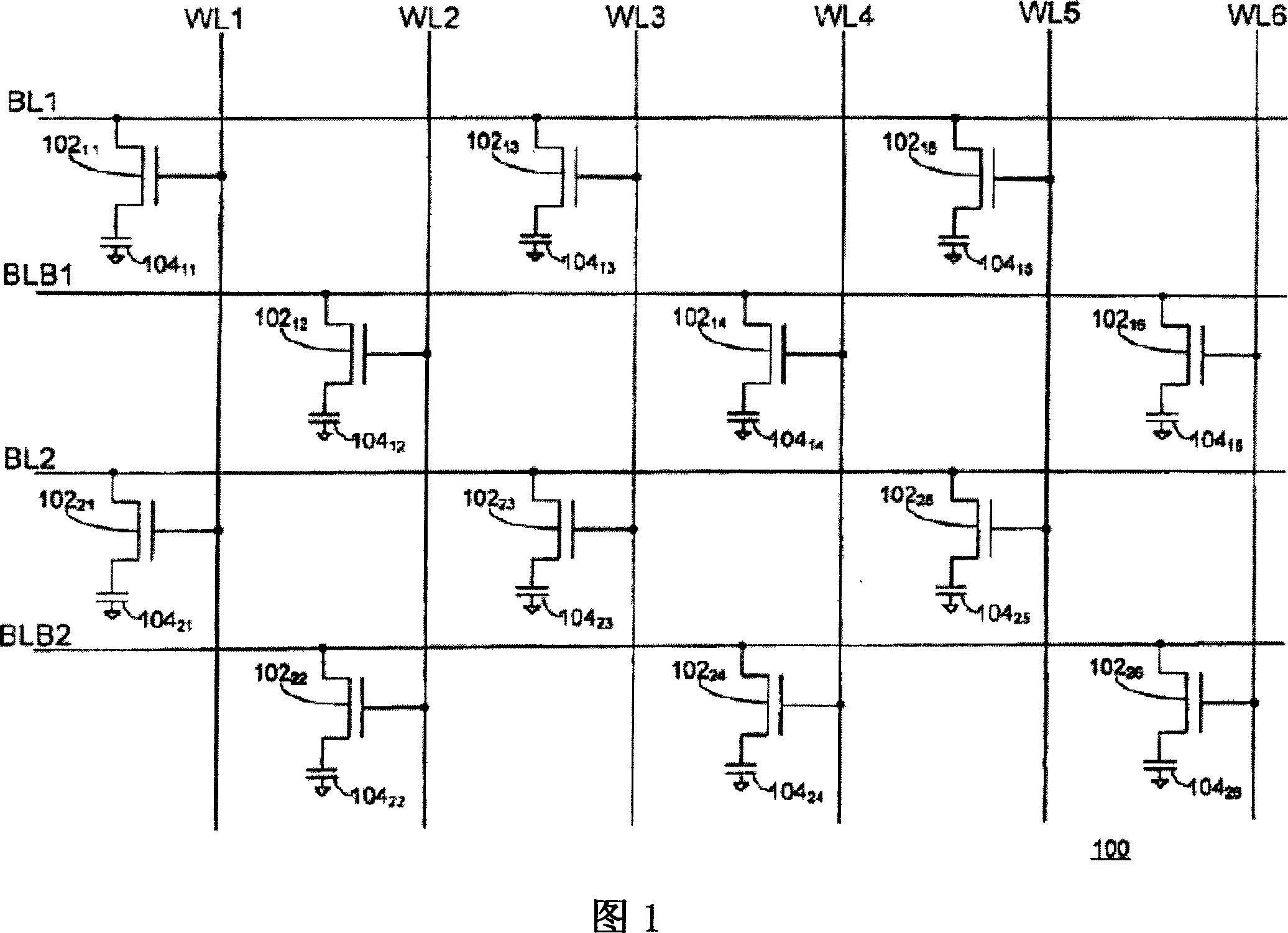
Figure 1 
Figure 2 
Figure 3
Abstract
Description
technical field
[0001] The present invention relates to the field of integrated circuit (IC) memory devices, including dynamic random access memory (DRAM) devices and other integrated circuit devices incorporating embedded dynamic random access memory. In particular, it relates to a shielded bit line structure for a dynamic random access memory array. Background technique
[0002] There are a variety of DRAM base devices or integrated circuits with embedded memory arrays, including Extended Data Output (EDO) DRAM, Synchronous DRAM (SDRAM), Double Data Rate (DDR) DRAM Random Access Memory, DDR3 Dynamic Random Access Memory (DDR3 DRAM), and the like. Regardless of configuration, the main purpose of DRAM is to store data. The main function of the memory is that data can be written into the memory, read from it or updated periodically to maintain the integrity of the stored data. In today's high-density designs, each DRAM cell typically consists of a single access transistor ...
Examples
Embodiment Construction
[0054] Referring to FIG. 1 , it is a part of a typical DRAM array 100 with a folded bit line structure, wherein the bit lines marked as BLB (bitline bar, such as BLB1 and BLB2) serve as the bit lines marked as BL (such as BL1 and BL2) Line reference, which is input to a sense amplifier (not shown) when the word line (WL) is "high".
[0055] Each memory cell of the DRAM array 100 includes an N-type channel access transistor 102 11 ~102 16 and 102 21 ~102 26 , and respectively include a connected storage capacitor 104 11 ~104 16 and 104 21 ~104 26 . The drain of each transistor 102 is coupled to one of the corresponding complementary bit lines, its gate is coupled to one of the word lines WL1-WL6, the source of each transistor 102 is coupled to the plate of the corresponding capacitor 104, the other plate of which Depending on the memory technology used, it is decided to couple to circuit ground (VSS) or to a common plate line.
[0056] In the part of the dynamic random...