
Semiconductor device having input/output sense amplifier for multiple sampling
a technology of sensing amplifier and semiconductor device, which is applied in the direction of information storage, static storage, digital storage, etc., can solve the problems of unnecessarily increasing the margin between the column selection line csl and the frp, and the data read operation may fail, etc., to achieve stably read
Patent Information
- Authority / Receiving Office
- US · United States
- Patent Type
- Applications(United States)
- Current Assignee / Owner
- Publication Date
- 2005-04-28
- Estimated Expiration
- Not applicable · inactive patent
Smart Images
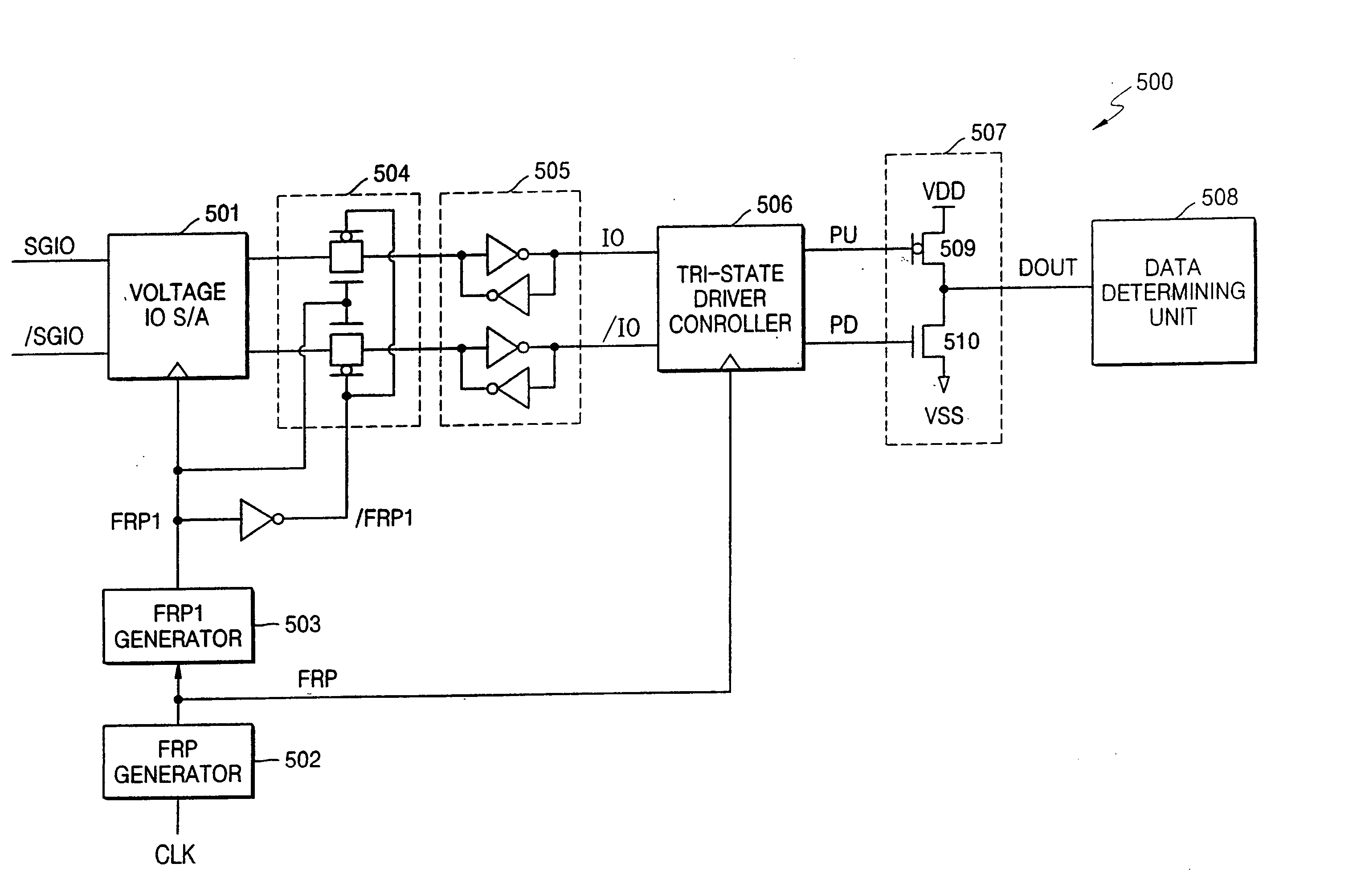
Figure 1 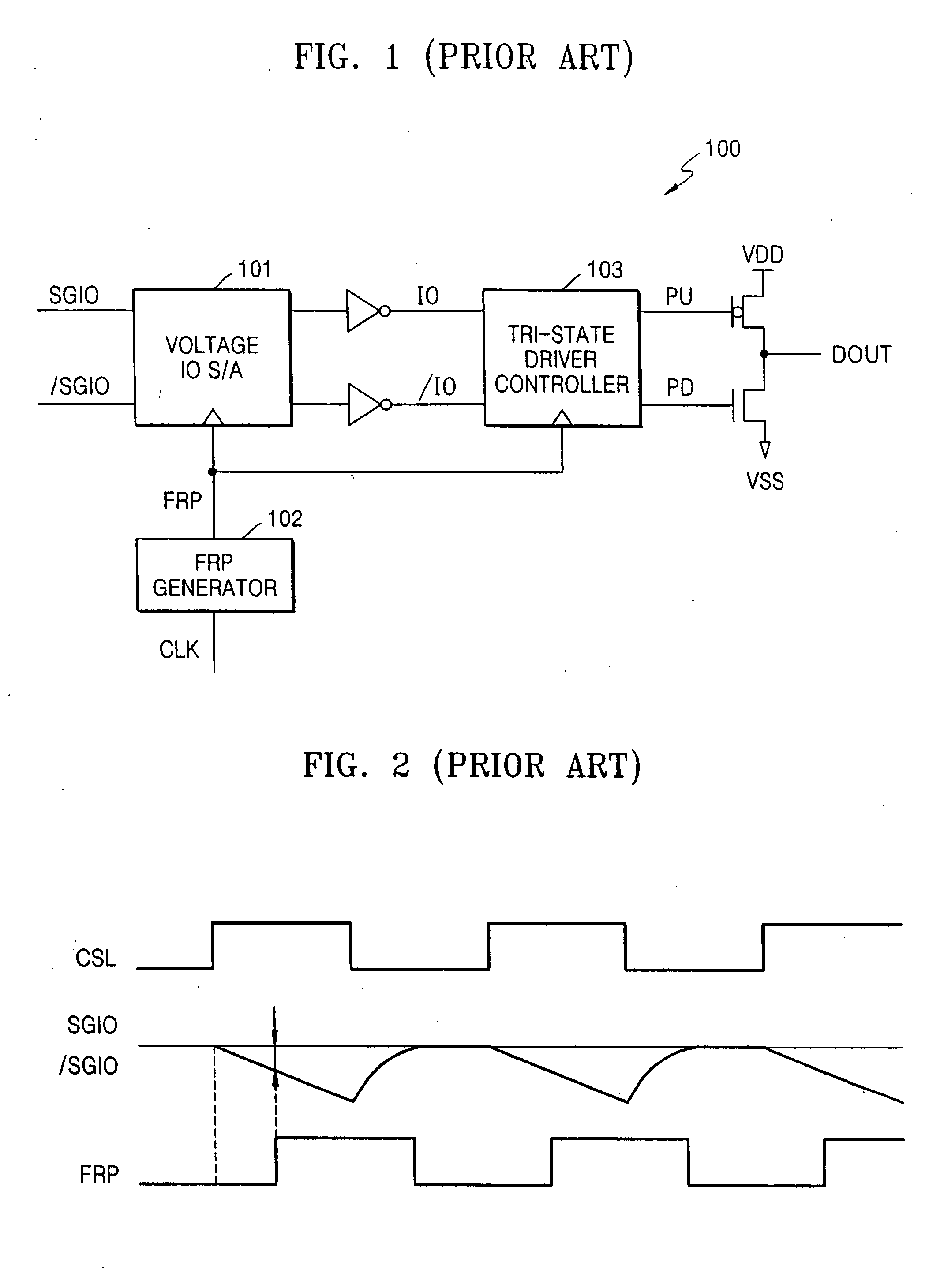
Figure 2 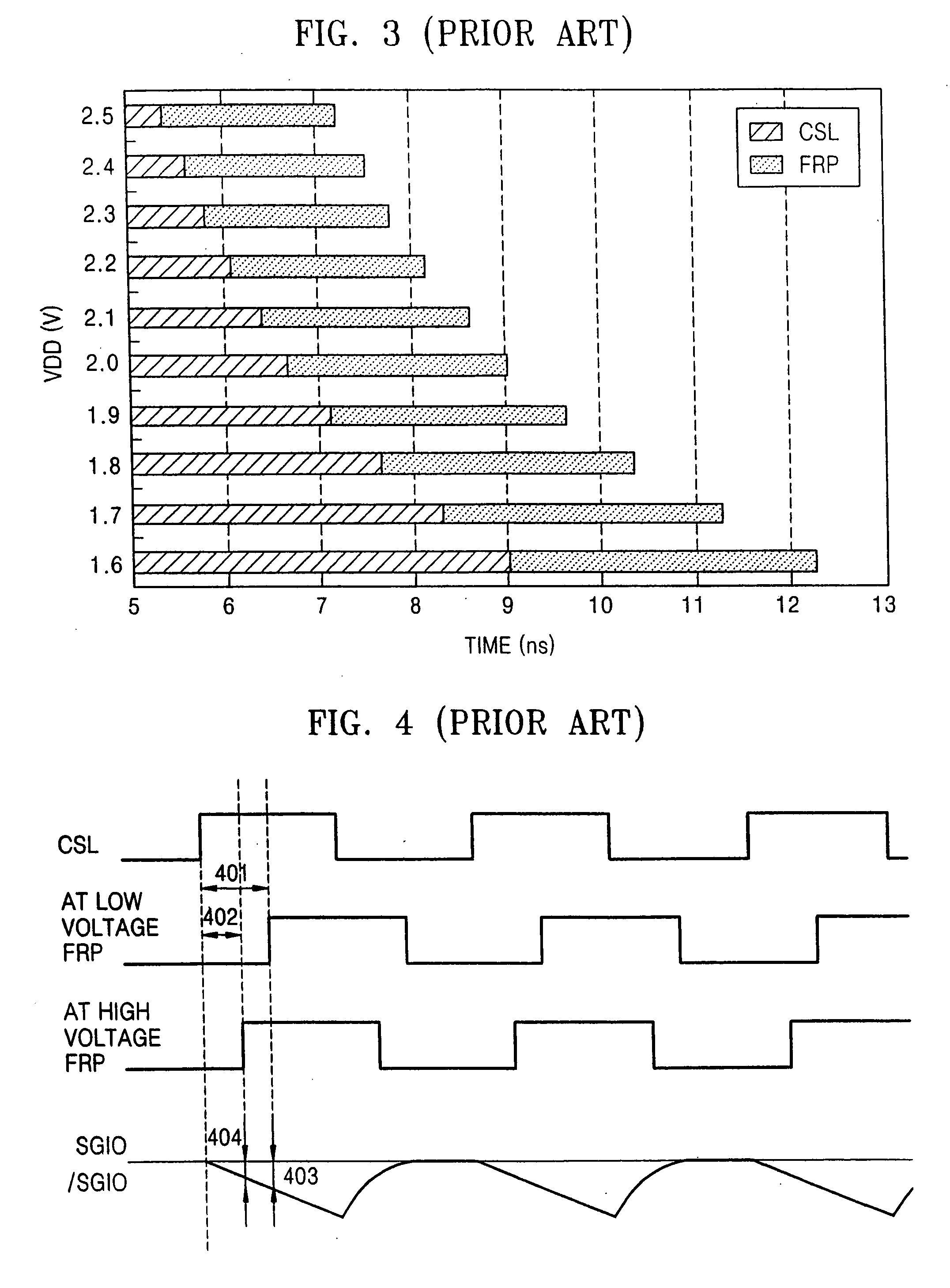
Figure 3
Abstract
Description
CROSS REFERENCE TO RELATED APPLICATION
[0001] This application claims the priority of Korean Patent Application No. 2003-75633, filed on Oct. 28, 2003, in the Korean Intellectual Property Office, the disclosure of which is hereby incorporated by reference in its entirety. BACKGROUND OF THE INVENTION
[0002] 1. Field of the Invention
[0003] The present invention relates to a semiconductor device, and more particularly, to a semiconductor device that is insensitive to a change in a voltage, circuit dimension or temperature, and provides for a rapid read data operation.
[0004] 2. Description of the Related Art
[0005] With the demand for semiconductor devices with increased speed, clock frequencies of the semiconductor devices increase and time intervals between signals decrease.
[0006] Also, as the amount of time necessary for data read and write operations decreases, more accurate data read and write operations are required.
[0007] In particular, in the case of semiconductor devices, a...
Examples
Embodiment Construction
[0051] The present invention will now be described more fully with reference to the accompanying drawings, in which exemplary embodiments of the invention are shown. Throughout the drawings, like reference numerals are used to refer to like elements.
[0052]FIG. 5 illustrates a data output circuit 500 of a semiconductor device according to a first exemplary embodiment of the present invention. The data output circuit 500 shown in FIG. 5 is a type of wave pipeline processor. As the operating speed of semiconductor devices increases, a column address strobe (CAS) latency increases. To implement a long CAS latency between 5 and 6 in a semiconductor device that operates at a high speed, a data output circuit that is a type of wave pipeline processor is widely used.
[0053] Referring to FIG. 5, the data output circuit 500 includes a voltage input / output (IO) sense amplifier (S / A) 501, a first read signal (FRP) generator 502, a second read signal (FRP1) generator 503, a transmission circuit...