
Multilayer type test board assembly for high-precision inspection
Patent Information
- Authority / Receiving Office
- US · United States
- Current Assignee / Owner
- Publication Date
- 2008-07-10
Smart Images
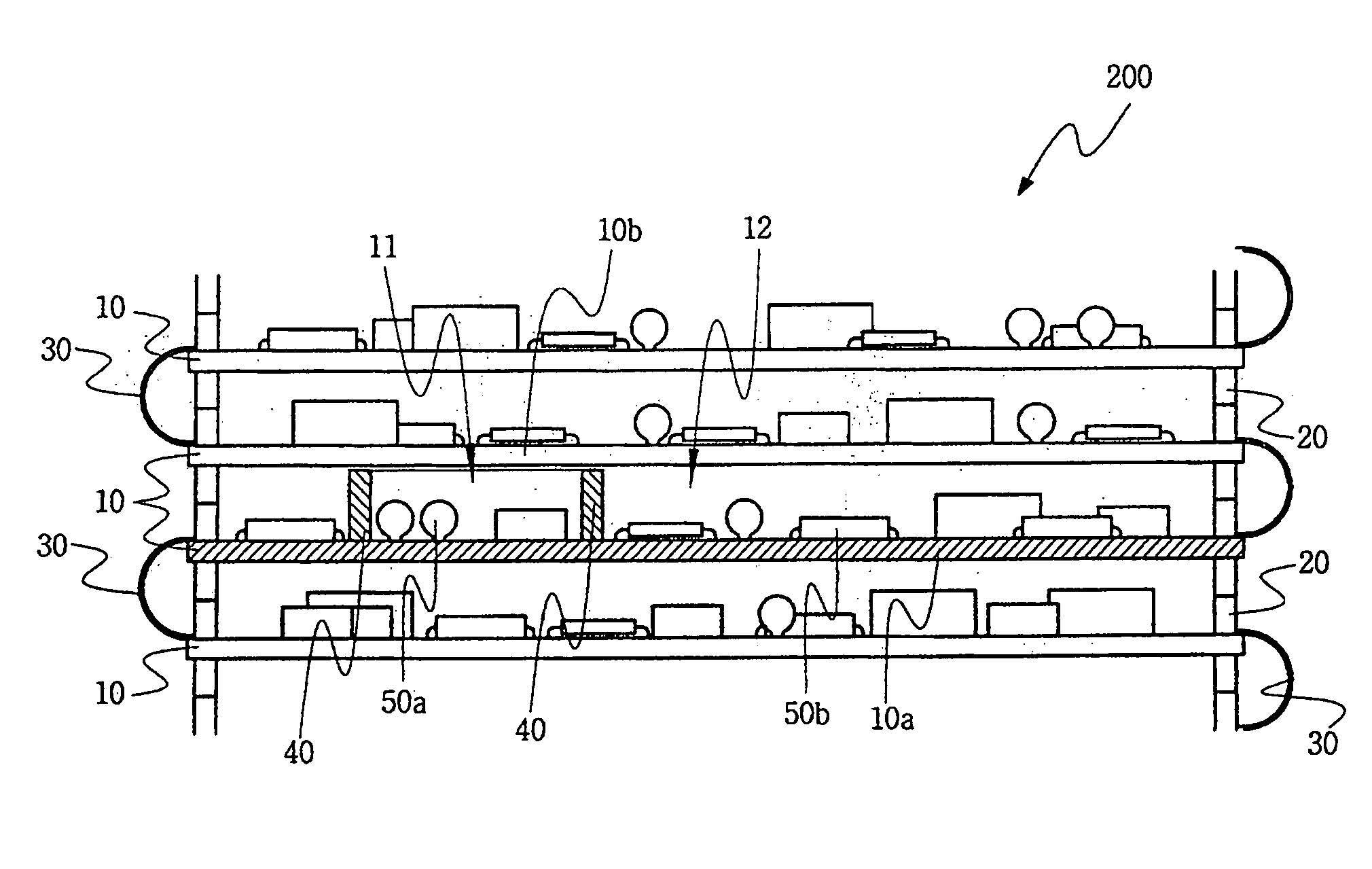
Figure 1 
Figure 2 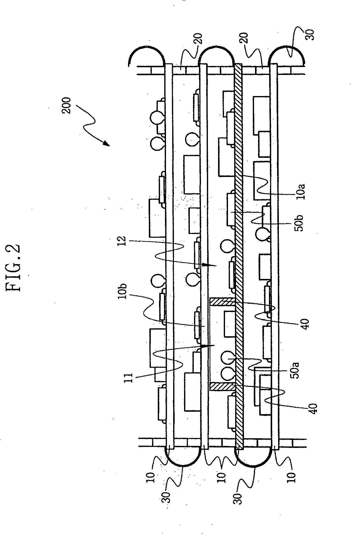
Figure 3
Abstract
Description
CROSS-REFERENCE TO RELATED APPLICATION
[0001] This application claims the benefit of Korean Patent Application No. 10-2007-0000933, filed in the Korean Intellectual Property Office on Jan. 4, 2007, the contents of which are hereby incorporated herein by reference in their entirety.BACKGROUND OF THE INVENTION
[0002] 1. Field of the Invention
[0003] The present invention relates to a multilayer type test board assembly for high-precision inspection, and more particularly to a test board assembly for high-precision inspection capable of measuring a micro current and a low current by safely protecting the test board assembly from an influence of external signals.
[0004] 2. Description of the Related Art
[0005] In general, a semiconductor device is manufactured by a fabrication process that includes forming patterns on a wafer and an assembling process that includes assembling the wafer having the patterns into unit chips.
[0006] An electric die sorting (EDS) process is performed between the fabrica...
Examples
Embodiment Construction
[0043]A multiplayer type test board assembly according to the present invention will now be described more fully hereinafter with reference to the accompanying drawings, in which exemplary embodiments of the invention are shown. This invention may, however, be embodied in different forms and should to not be construed as limited to the embodiments set forth herein.
[0044]It will also be understood that when an element such as a layer, region or substrate is referred to as being on another element, it can be directly on the other element or intervening elements may also be present, or it can be partially or completely in the other element. In contrast, if an element is referred to as being directly on another element, then no other intervening elements are present.
[0045]FIG. 2 is a schematic side sectional view of a multilayer type test board assembly 200 for high-precision inspection according to an embodiment of the present invention.
[0046]As shown in FIG. 2, a multilayer type test ...