
Light receiving element
Patent Information
- Authority / Receiving Office
- US · United States
- Current Assignee / Owner
- Publication Date
- 2009-03-26
- Estimated Expiration
- Not applicable · inactive patent
Smart Images
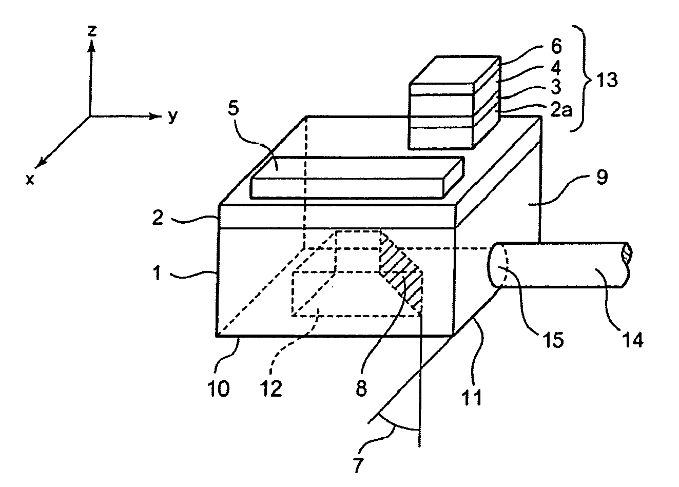
Figure 1 
Figure 2 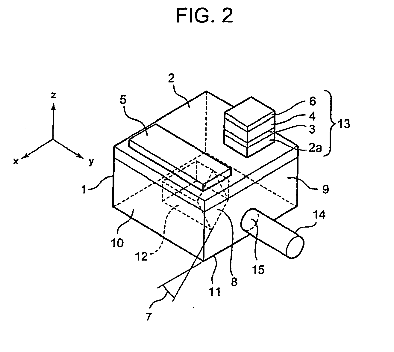
Figure 3
Abstract
Description
[0001] This application is based upon and claims the benefit of priority from Japanese Patent Application No. 2007-245660 filed on Sep. 21, 2007, the content of which are incorporated by reference.BACKGROUND ART
[0002] 1. Technical Field
[0003] The present invention relates to an edge illuminated type light receiving element.
[0004] 2. Description of the Related Art
[0005] With the advancement of technology in recent years, edge illuminated type light receiving elements having various reflection structures have been developed. For example, a combination use of an edge illuminated type light receiving element with a planner lightwave circuit is disclosed in a Non-Patent Document in URL: http: / / www.kyosemi.co.jp / product / data / ja2 / KPE12GC.html, “Optical Communication Component,” [online], by Kyosemi Corporation (search date: Sep. 10, 2007). Specifically, the Non-Patent Document describes an edge illuminated type light receiving element having a structure in which light enters an edge surface per...
Examples
first exemplary embodiment
1. First Exemplary Embodiment
[0015]An n-type cladding layer 2 having a composition of Inx1Ga (1-x1) Asy1P (1-y1) is disposed on the top surface of an n-type InP substrate 1. This n-type cladding layer 2 has an n-type cladding layer 2a protruding in a mesa type structure on a predetermined region of the top surface of the n-type cladding layer 2. On the top surface of the n-type cladding layer 2a, an optical absorption layer 3 of a pure semiconductor having a composition of Inx2Ga (1-x2) Asy2P (1-y2) is disposed. On the top surface of the optical absorption layer 3, a p+ type cladding layer 4 having a composition of, Inx3Ga (1-x3) Asy3P (1-y3) is disposed. An electrode 6 is disposed on the top surface of the p+ type cladding layer 4. An electrode 5 is disposed on a region of the top surface of the n-type cladding layer 2, the region being different from the region on which the n-type cladding layer 2a is disposed. The n-type cladding layer 2a, the optical absorption layer 3, the p+ t...
second exemplary embodiment
2. Second Exemplary Embodiment
[0020]Hereinafter, means for solving the problems will be described by use of the reference numerals used in “EXEMPLARY EMBODIMENTS” with parentheses. These reference numerals are added for clarifying correspondences of the description in “What is claimed is” and the description in “EXEMPLARY EMBODIMENTS.” However, these reference numerals should not be used for interpretation of the technical scope of the present invention described in “What is claimed is.”
[0021]The light receiving element according to the present invention includes a substrate (1), a light receiver (13) that is formed on the top surface of the substrate and absorbs light, and a reflector (8) that reflects light in a direction of the light receiver, the light being entered from a side surface (9) of the substrate. In a cross section (10) in parallel with the top surface of the substrate, a reflective surface of the reflector (8) is inclined with respect to the side surface (9).
[0022]Ac...