
Organic light emitting device
a light-emitting device and organic technology, applied in the direction of discharge tube luminescnet screens, discharge tube/lamp details, electric discharge lamps, etc., can solve the problems of power consumption reduction, limited efficiency and lifetime improvement of conventional organic light-emitting devices, etc., to improve light-emitting efficiency and lifetime, reduce power consumption, and improve driving voltage
Patent Information
- Authority / Receiving Office
- US · United States
- Patent Type
- Applications(United States)
- Current Assignee / Owner
- Publication Date
- 2009-07-02
- Estimated Expiration
- Not applicable · inactive patent
Smart Images
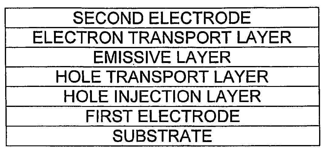
Figure 1 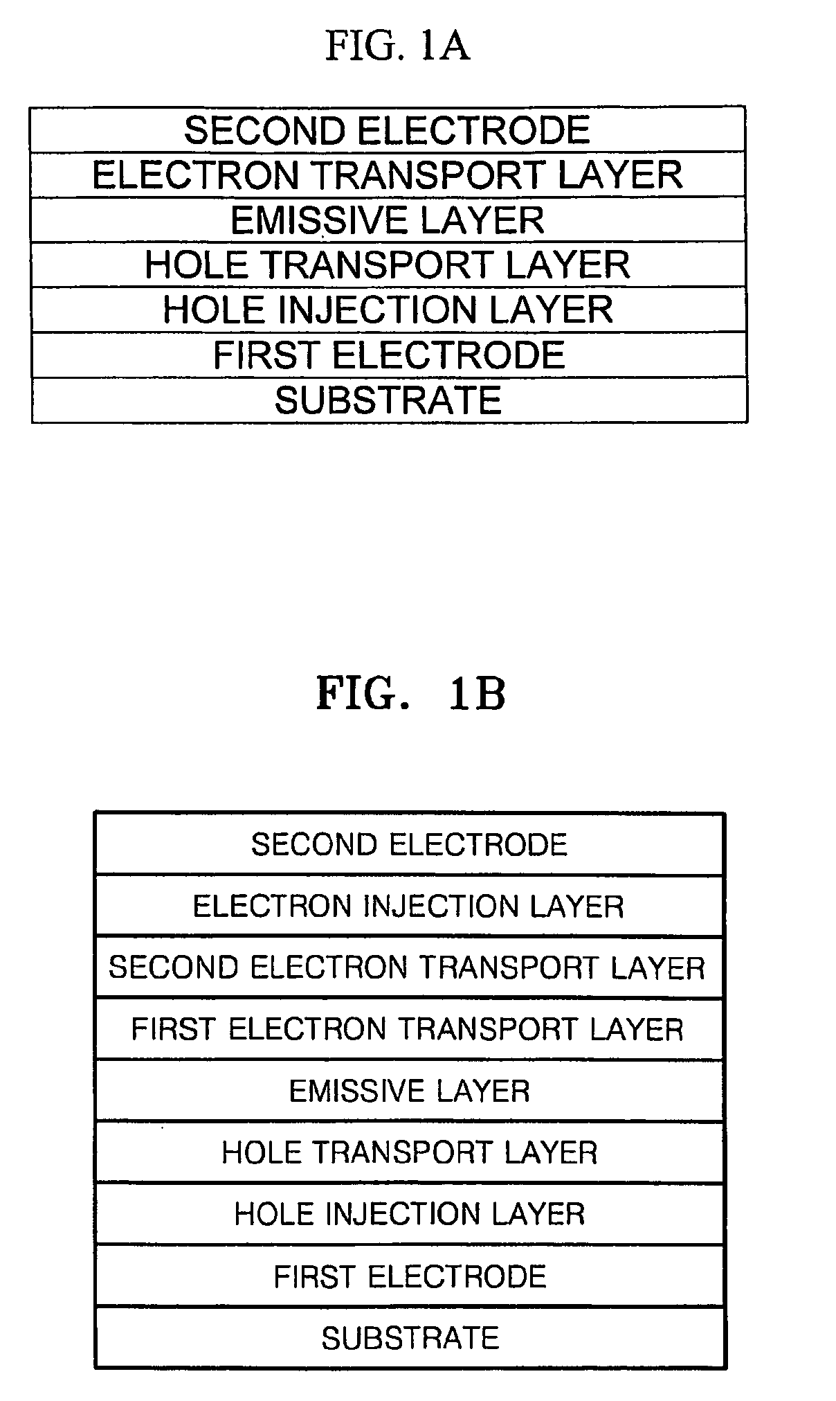
Figure 2 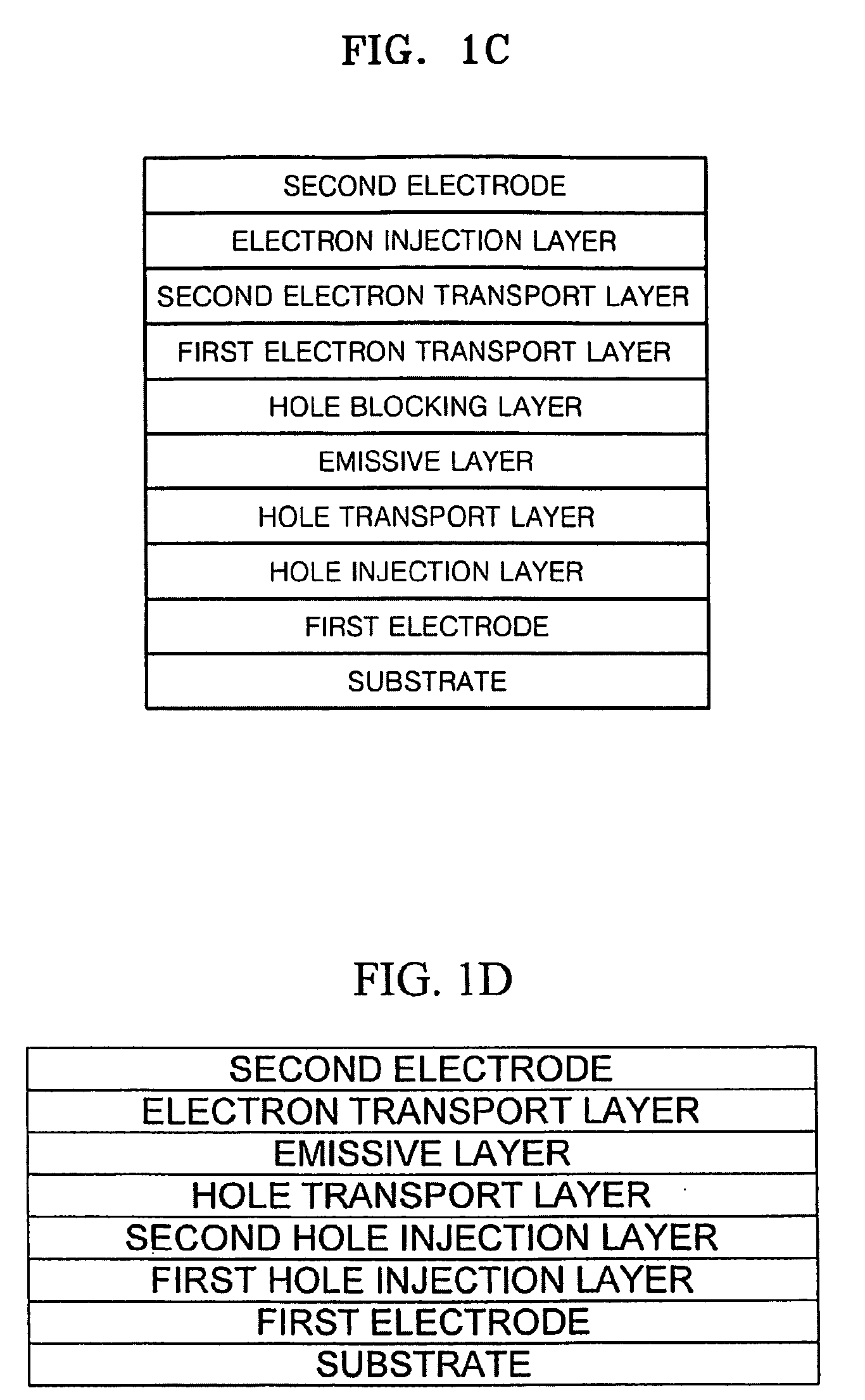
Figure 3
Abstract
Description
CROSS-REFERENCE TO RELATED APPLICATION
[0001] This application claims the benefit of Korean Application No. 2007-140555, filed Dec. 28, 2007, in the Korean Intellectual Property Office, the disclosure of which is incorporated herein by reference.BACKGROUND OF THE INVENTION
[0002] 1. Field of the Invention
[0003] Aspects of the present invention relate to an organic light emitting device, and more particularly, to an organic light emitting device with improved driving voltage, light emitting efficiency, lifetime, and the like by using a novel hole injecting material and a novel electron transporting material. In addition, aspects of the present invention may contribute to development of a high image quality organic light emitting device, and provide an organic light emitting device with reduced power consumption and improved lifetime.
[0004] 2. Description of the Related Art
[0005] Organic light emitting devices are devices in which, when a current is supplied to an organic layer interposed be...
Examples
example 1
Manufacture of Organic Light Emitting Device
[0067]As an anode, a Corning 15 Ω / cm2 (1200 Å) ITO glass substrate was cut to a size of 50 mm×50 mm×0.7 mm, and was ultrasonically washed with isopropyl alcohol and pure water for 5 minutes, respectively. The ITO glass substrate was irradiated with ultraviolet rays for 30 minutes and washed with ozone.
[0068]Then, molybdenum oxide and NPB were co-deposited on the substrate to form a first hole injection layer with a thickness of 100 Å. Subsequently, F16-TCNQ was coated on the first hole injection layer to form a second hole injection layer.
[0069]NPB was vacuum deposited on the second hole injection layer to form a hole transport layer having a thickness of 60 nm. After the formation of the hole transport layer, 100 parts by weight of Alq3 as a host and 5 parts by weight of C545T as a dopant were vacuum deposited on the hole transport layer to form an emissive layer.
[0070]Then, 50 parts by weight of LiF and 50 parts by weight of BeBq2 were v...
example 2
Manufacture of Organic Light Emitting Device
[0072]An organic light emitting device was manufactured in the same manner as in Example 1, except that 50 parts by weight of lithium quinolate and 50 parts by weight of BeBq2 were vacuum co-deposited to form the electron transport layer.
example 3
Manufacture of Organic Light Emitting Device
[0073]As an anode, a Corning 15 Ω / cm2 (1200 Å) ITO glass substrate was cut to a size of 50 mm×50 mm×0.7 mm, and was ultrasonically washed with isopropyl alcohol and pure water for 5 minutes, respectively. The ITO glass substrate was irradiated with ultraviolet rays for 30 minutes and washed with ozone.
[0074]A hole injection layer formed of CuPc was formed on the substrate to a thickness of 10 nm.
[0075]NPB was vacuum deposited on the hole injection layer to form a hole transport layer having a thickness of 60 nm. After the formation of the hole transport layer, 100 parts by weight of Alq3 as a host and 5 parts by weight of C545T as a dopant were vacuum deposited on the hole transport layer to form an emissive layer.
[0076]Then, Bebq2 was vacuum deposited on the emissive layer to form a first electron transport layer (ETL1) having a thickness of 10 nm.
[0077]30 parts by weight of LiF and 70 parts by weight of Bebq2 were vacuum co-deposited on ...