
CMOS back-gated keeper technique
a backgated keeper and keeper technology, applied in the field of very large scale semiconductor integrated (vlsi) circuits and technology, can solve the problems of negative affecting the timing precision of deep submicron vlsi logic circuits, incomplete transition voltages presented at output buffers, and excessive crowbar current in buffer side, so as to reduce leakage currents and improve noise immunity.
Patent Information
- Authority / Receiving Office
- US · United States
- Patent Type
- Applications(United States)
- Current Assignee / Owner
- Publication Date
- 2009-09-10
- Estimated Expiration
- Not applicable · inactive patent
Smart Images
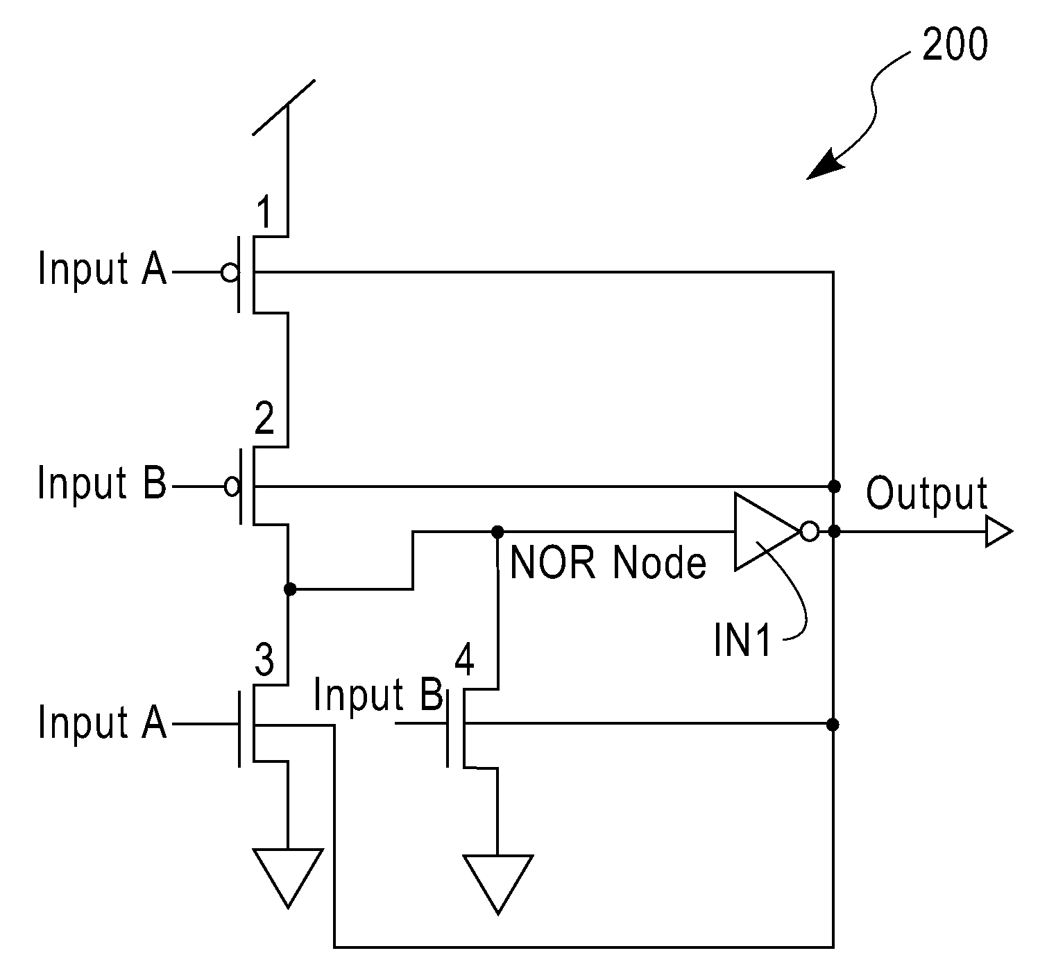
Figure 1 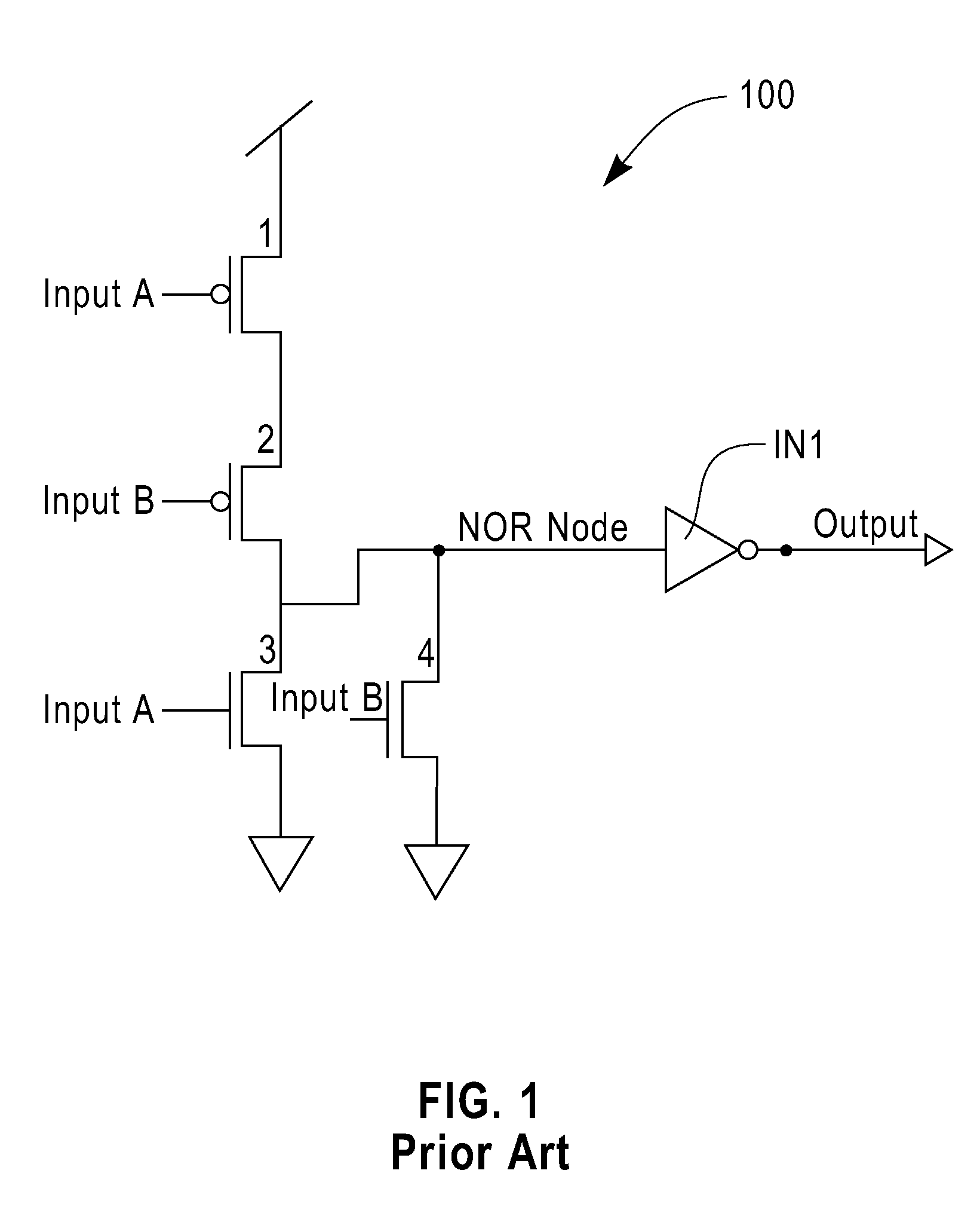
Figure 2 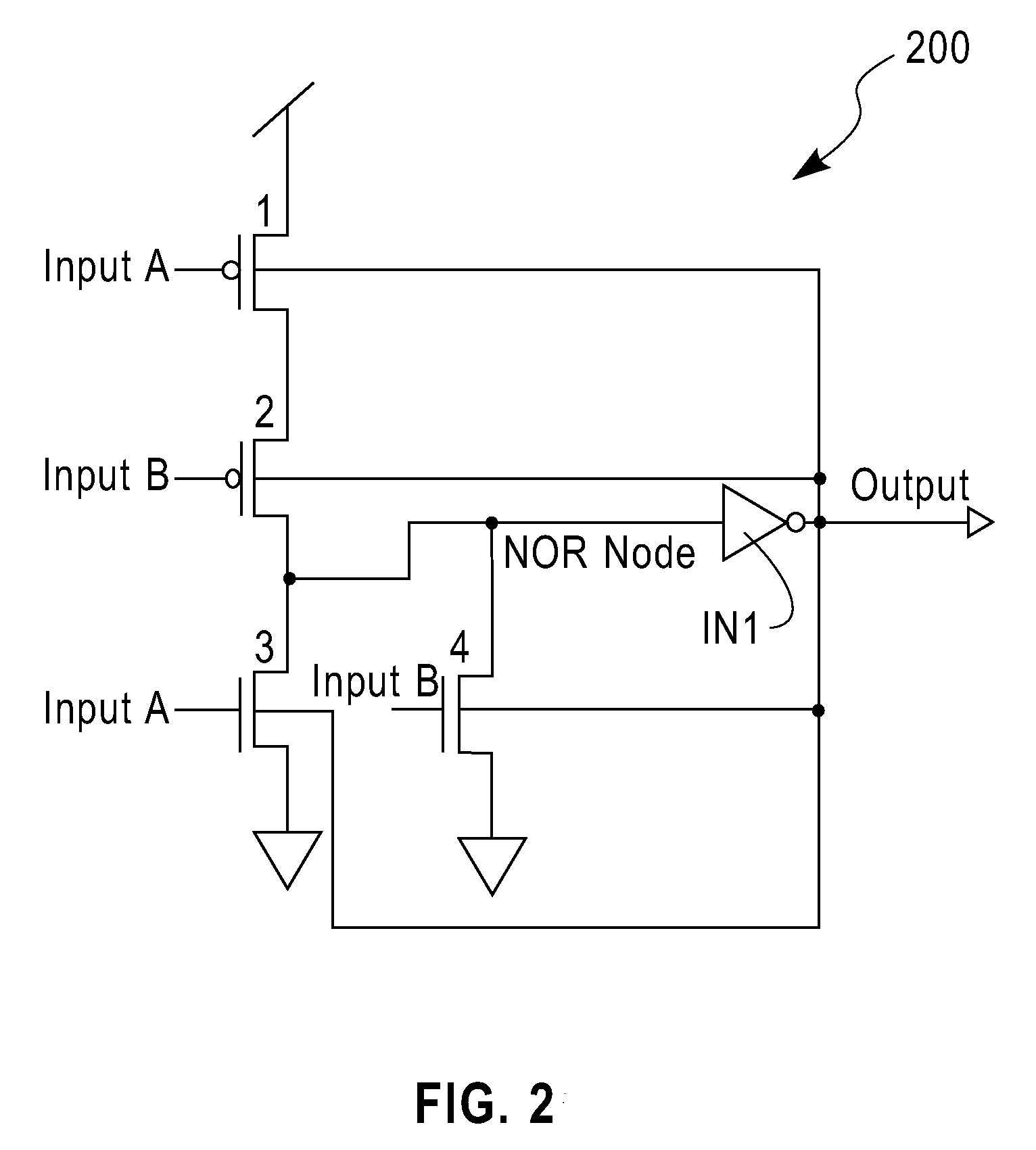
Figure 3
Abstract
Description
BACKGROUND OF THE INVENTION
[0001] The present invention relates to very large scale semiconductor integrated (VLSI) circuits and technology, and more particularly relates to VLSI circuitry designed with the back-gated MOSFET devices in such a way that their threshold voltages are dynamically modulated during circuit operation to realize improved logic state capture, reduced leakage current and improved noise immunity at the back-gated devices.
[0002] The need for low-power VLSI circuitry for use in numerous electronic applications is ever growing. To reduce power consumption, lower operating voltages (Vdd) and minimized device dimensions are the constant aim of IC designers. To lower the threshold voltage (VTh) and the operational voltage for IC devices, silicon-on-oxide (SOI) MOSFETs have been developed and are known. Fuse, et al., “0.5 V SOI CMOS Pass-Gate Logic,” DIGEST OF TECHNICAL PAPERS, IEEE International Solid-State Circuits Conference; vol. 39, February 1996; pp. 88-89.
[0003] S...
Examples
Embodiment Construction
[0024]As mentioned above, the inventive back-gated operation contemplated by the invention may be implemented in any known combinatory logic circuit topology by merely placing a minimum sized inverter on the combinatorial logic circuit output, the output of which is then arranged to drive the back gates of all circuit devices. The effect of the inverted output driving the back gates of all circuit devices is, like DTCMOS, to lower the relative threshold of the “on” device, and elevate the relative threshold of the “off” device. The result is that the “on” devices are on harder, and the leakage of “off” devices is clamped harder thereby improving noise immunity.
[0025]To highlight the inventive operation, attention is directed to prior art FIG. 1, which is a schematic representation of a simple 2-way OR circuit 100 implemented in standard, static combinatorial CMOS technology. Prior art OR circuit 100 comprises a first PMOS device 1 having a gate input A, a source that may be connecte...