
Solid-state image device manufacturing method thereof, and image capturing apparatus
a manufacturing method and solid-state image technology, applied in the direction of radio frequency controlled devices, instruments, material analysis, etc., can solve the problems of difficult to realize the stress liner technique used in the high-speed mos logic process and the technique which reduces the noise of the cmos image sensor portion, so as to improve the mobilities of the mos transistors, improve the operation speed, and improve the mobility of the individual transistors of the peripheral circuit portion of the solid-state image device
Patent Information
- Authority / Receiving Office
- US · United States
- Patent Type
- Applications(United States)
- Current Assignee / Owner
- Publication Date
- 2010-09-09
Smart Images
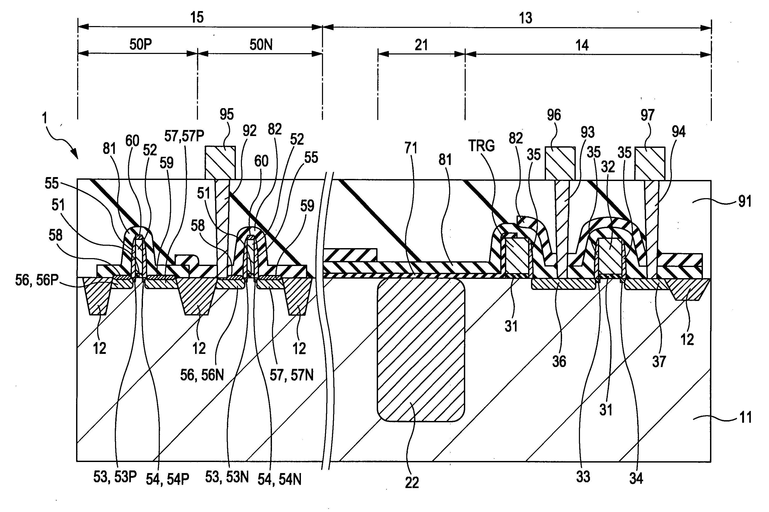
Figure 1 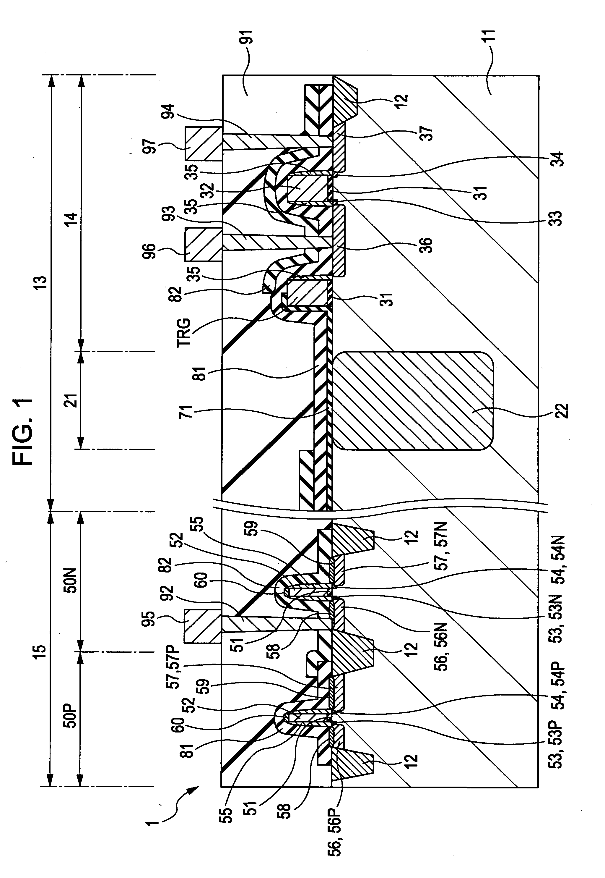
Figure 2 
Figure 3
Abstract
Description
BACKGROUND OF THE INVENTION
[0001] 1. Field of the Invention
[0002] The present invention relates to a solid-state image device, a manufacturing method thereof, and an image capturing apparatus.
[0003] 2. Description of the Related Art
[0004] In recent years, a CMOS image sensor has been widely used for a video camera, a mobile phone, and the like. In addition, since the CMOS sensor can be formed using a CMOS logic-LSI manufacturing process as a base process, power consumption can be decreased as compared to that of a CCD image sensor having a high voltage analog circuit. Furthermore, since the CMOS image sensor can be microfabricated, mass production thereof can be advantageously performed at a low cost. In addition, in a substrate in which the CMOS image sensor is formed, a logic circuit can be incorporated by the same manufacturing process as that of the CMOS image sensor; hence, on-chip fabrication of an image-data processing circuit can also be realized. Accordingly, when the CMOS imag...
Examples
first embodiment
1. First Embodiment
First Example of the Structure of a Solid-State Image Device
[0051]A first example of the structure of a solid-state image device according to a first embodiment of the present invention will be described with reference to a schematic cross-sectional structural view of FIG. 1.
[0052]As shown in FIG. 1, an element isolation region 12 which isolates a photoelectric conversion portion 21, a pixel transistor portion 14, a peripheral circuit portion 15, and the like is formed in a semiconductor substrate 11, these portions 21 and 14 forming a pixel portion 13. As the semiconductor substrate 11, for example, a silicon substrate is used. Of course, a silicon-on-insulator (SOI) substrate may also be used. The element isolation region 12 is formed to have a shallow trench isolation (STI) structure. In addition, the periphery of the photoelectric conversion portion 21 and the periphery of the pixel transistor portion 14 each may also have an STI structure. Alternatively, the ...
application example 1
of the Solid-State Image Device
[0115]Next, an application example of the solid-state image device 1 will be described.
[0116]First, a structural example in which one pixel is output by one pixel transistor portion will be described with reference to a plan layout view of FIG. 7A and an equivalent circuit diagram of FIG. 7B.
[0117]As shown in FIGS. 7A and 7B, the structure is formed of one photoelectric conversion portion 21 (photodiode 22) and the pixel transistor portion 14 which includes the transfer gate electrode TRG, the floating diffusion FD, a reset transistor RST, an amplifying transistor Amp, and a selection transistor SEL. This is a type in which the photodiode is not shared; however, of course, there are a type in which the photodiode is shared and a type in which a three-transistor structure is used instead of a four-transistor structure.
application example 2
of the Solid-State Image Device
[0118]Next, a so-called two-pixel shared structural example in which two pixels are output by one pixel transistor portion will be described with reference to a plan layout view of FIG. 8.
[0119]As shown in FIG. 8, this example is a so-called two-pixel shared structure, and two photoelectric conversion portions 21 (21A and 21B) are disposed. At the center of the arrangement of the photoelectric conversion portions 21, a floating diffusion portion FD is formed in an active region which is connected to the two photoelectric conversion portions 21. In addition, at the boundaries between the floating diffusion FD and the two photoelectric conversion portions 21, transfer gates TRG (TRG-A and TRG-B) are respectively formed. In regions adjacent to the photoelectric conversion portions 21, the pixel transistor portions 14 (14A and 14B) are each formed with the element isolation region 12 interposed therebetween. In this pixel transistor portion 14A, for exampl...