
Single photon avalanche diode for CMOS circuits
a technology of cmos circuit and single photon, which is applied in the field of single photon avalanche diodes, can solve problems such as inability to meet the requirements of production, achieve the effects of improving broad spectrum sensitivity, reducing circuit complexity, and improving blue respons
Patent Information
- Authority / Receiving Office
- US · United States
- Current Assignee / Owner
- Publication Date
- 2013-08-01
Smart Images
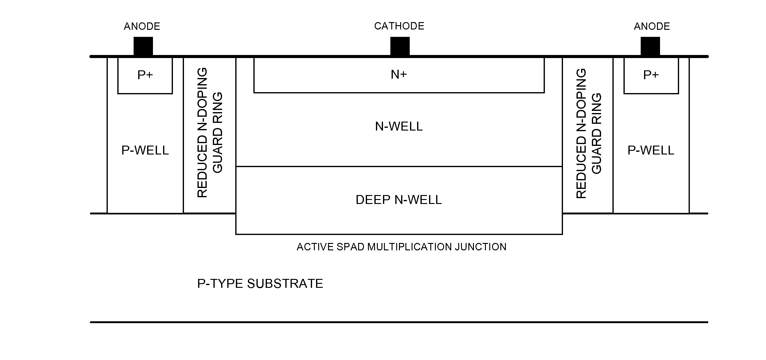
Figure 1 
Figure 2 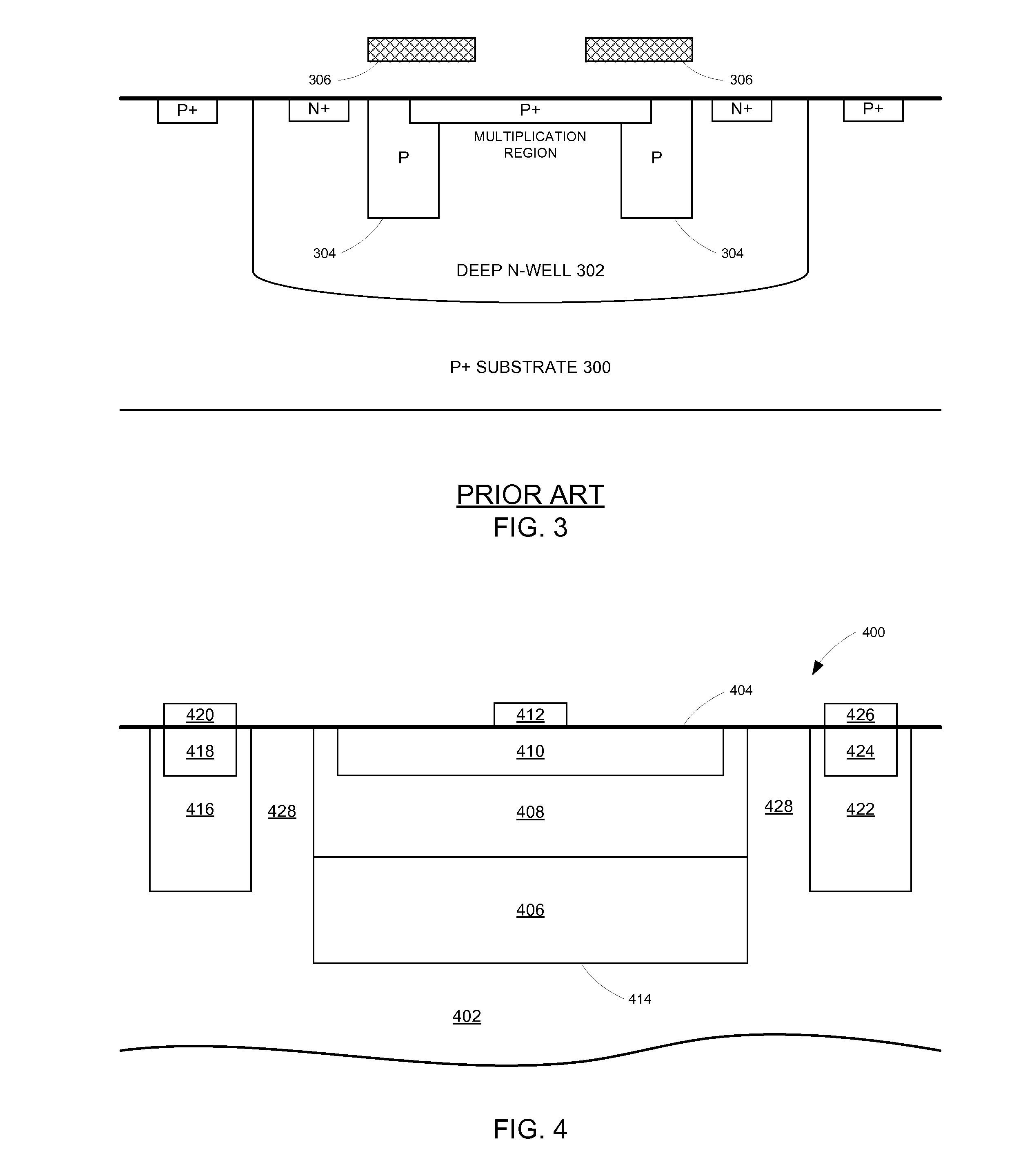
Figure 3
Abstract
Description
FIELD OF THE INVENTION
[0001] The present invention relates to a single photon avalanche diode (SPAD) and a method of fabricating same, and relates in particular to SPADs manufactured in a CMOS fabrication process.BACKGROUND TO THE INVENTION
[0002] Photodiodes convert light into electrical signals, and form the basis of a wide range of imaging and detection devices. Common configurations of photodiodes include PIN photodiodes, operated in photovoltaic or photoconductive mode, and single photon avalanche diodes (SPADs), typically operated in Geiger mode. Photodiodes can be realised using a number of different technologies, but it is particularly convenient and economical to form photodiodes using the CMOS fabrication process that has evolved as the production method of choice for integrated circuits of almost all types.
[0003] Some examples of a PIN photodiode formed in a CMOS fabrication process are given in Ciftcioglu et al, “Integrated Silicon PIN Photodiodes Using Deep N-Well in a Stan...
Examples
Embodiment Construction
[0097]In the foregoing description, it will be appreciated that the examples given with regard to p-type and n-type materials can apply equally if the conductivity types are reversed (that is, n-type material is replaced by p-type and vice versa) with appropriate reversals of voltages, anodes / cathodes and the like. Portions of this document assume a p-type substrate as this is mostly standard in CMOS integrated circuits.
[0098]FIG. 4 is a schematic of a first embodiment of a single photon avalanche diode (SPAD) that is fabricated as part of a CMOS integrated circuit 400. The SPAD 404 is formed in the epitaxial layer (‘epi-layer’) 402 that has been grown on a substrate (not shown). A deep well 406 is implanted into the epi-layer 402 and covered with a well of the same conductivity type 408 that is connected in turn to a heavily doped electrode implant 410 which is connected to the contact 412. An implant of opposite conductivity type 416, 422 is formed around a guard ring 428, with a ...