
Touch screen, method for producing touch screen, touch display device
Patent Information
- Authority / Receiving Office
- US · United States
- Current Assignee / Owner
- Publication Date
- 2016-03-17
Smart Images
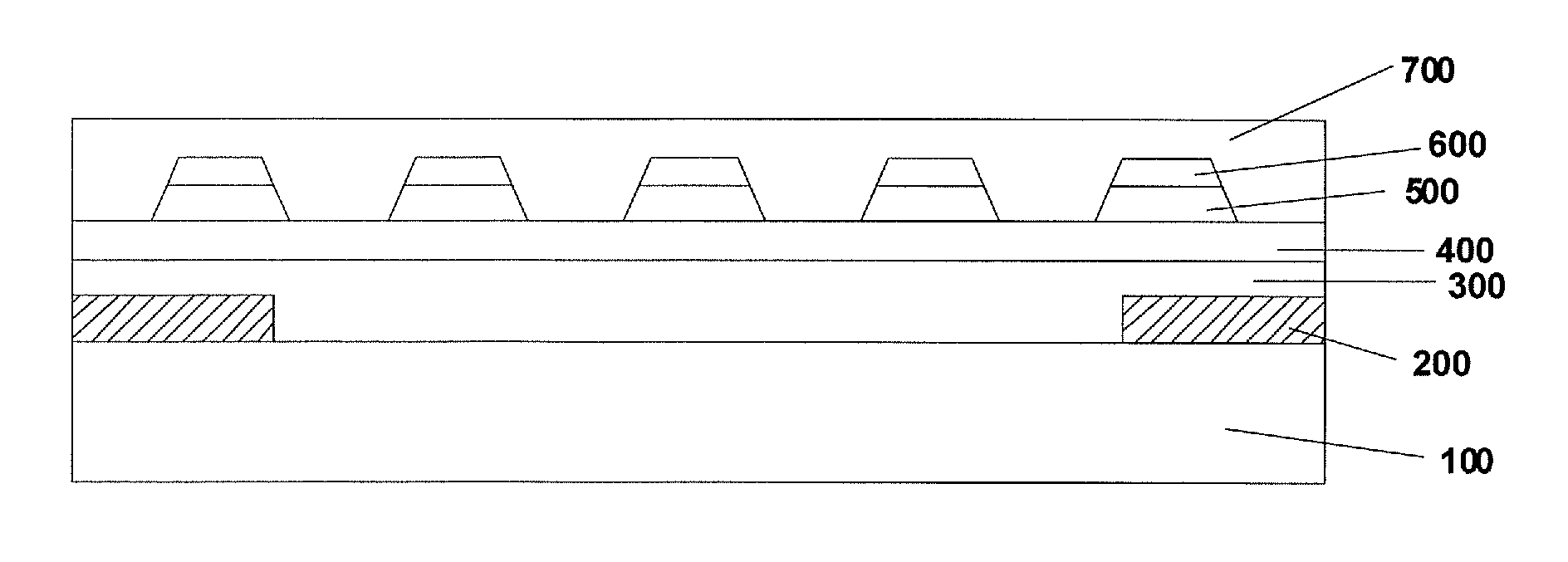
Figure 1 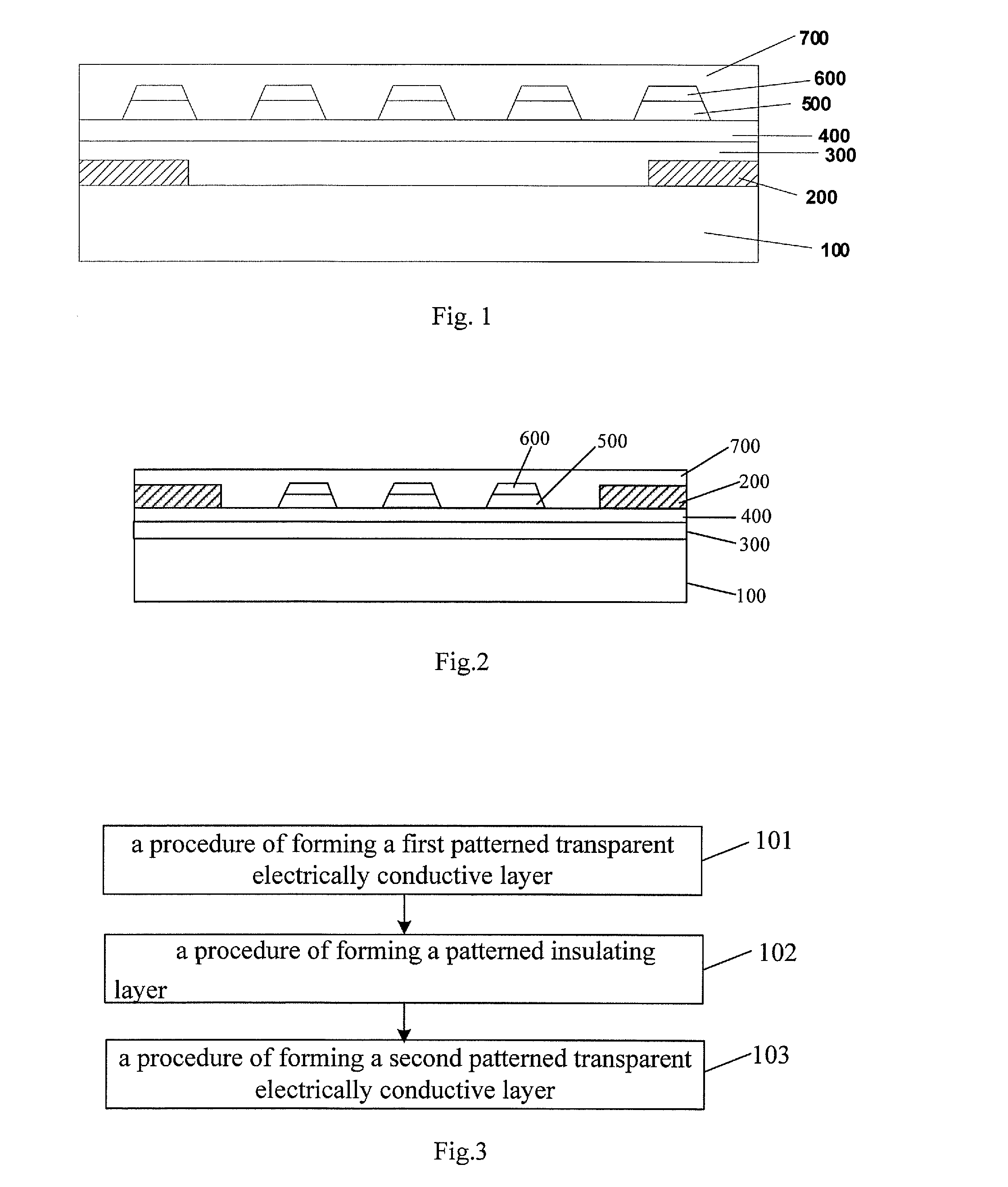
Figure 2 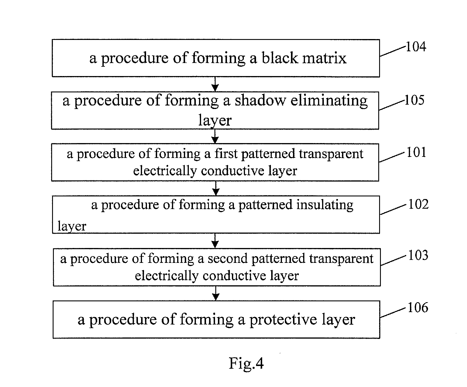
Figure 3
Abstract
Description
FIELD OF THE INVENTION
[0001] The present invention relates to the field of display technology, in particular relates to a touch screen, a method for producing the touch screen, and a touch display device.BACKGROUND OF THE INVENTION
[0002] Touch display has been developed rapidly and has gradually been developed into a main-trend flat-panel display. At present, the touch display is mostly manufactured by laminating a touch screen having touch control function to a display panel. And the touch screen is often of capacitive sensing, when a finger (or other object) approaches or touches the touch screen, it would influence the capacitance between a drive line and an induction line which intersect each other around a touch point. The position of the touch point can be identified by detecting a change in the capacitance between the drive line and the induction line.
[0003] With consumers' requirement for thinning of the touch display, technologists have developed many techniques to produce thi...
Examples
Embodiment Construction
[0040]Next, the technical solutions of the embodiments of the invention will be clearly and comprehensively described in combination with the figures of the embodiments of the invention. Obviously, the described embodiments are only part of the embodiments of the invention, rather than all of them.
[0041]An embodiment of the present invention provides a touch screen, and the sectional view thereof is shown in FIG. 1. The touch screen may comprise: a transparent substrate 100, a first patterned transparent electrically conductive layer 400, a patterned insulating layer 500, and a second patterned transparent electrically conductive layer 600, wherein the first patterned transparent electrically conductive layer 400, the patterned insulating layer 500 and the second patterned transparent electrically conductive layer 600 may be successively formed above the transparent substrate 100; among the first patterned transparent electrically conductive layer 400 and the second patterned transp...