
Thin film transistor array substrate and manufacturing method thereof
Patent Information
- Authority / Receiving Office
- US · United States
- Current Assignee / Owner
- Publication Date
- 2017-06-08
- Estimated Expiration
- Not applicable · inactive patent
Smart Images
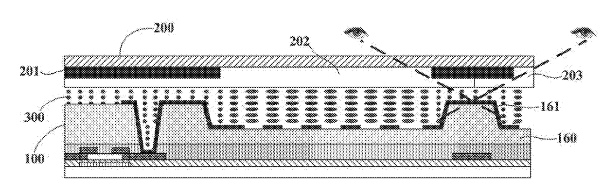
Figure 1 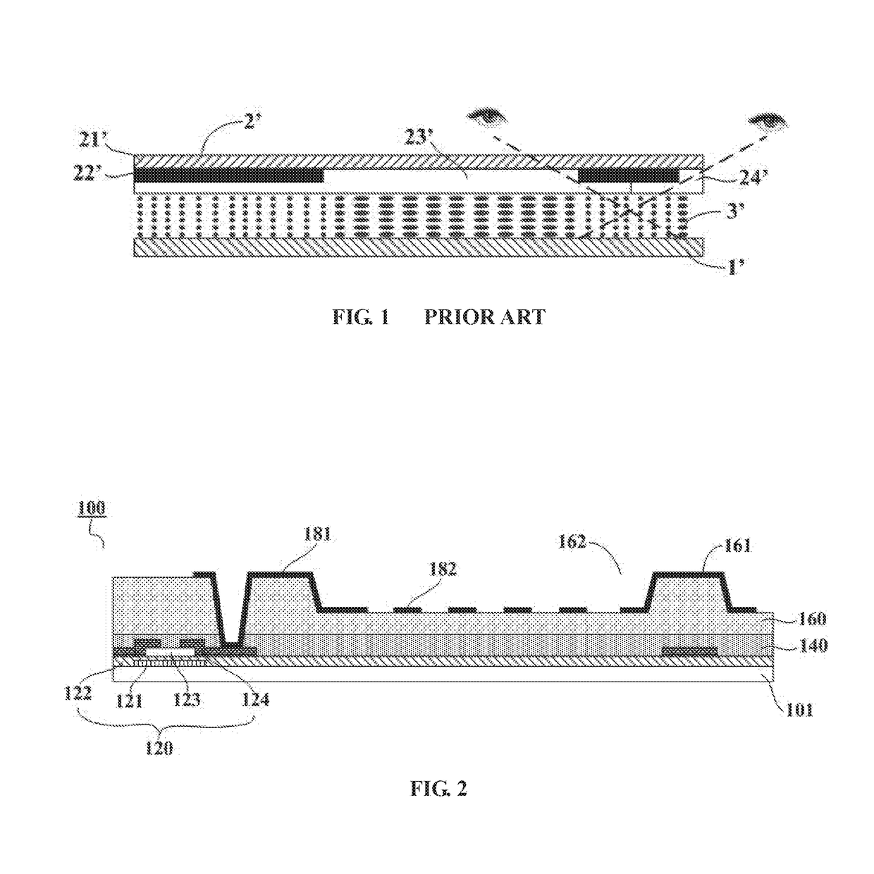
Figure 2 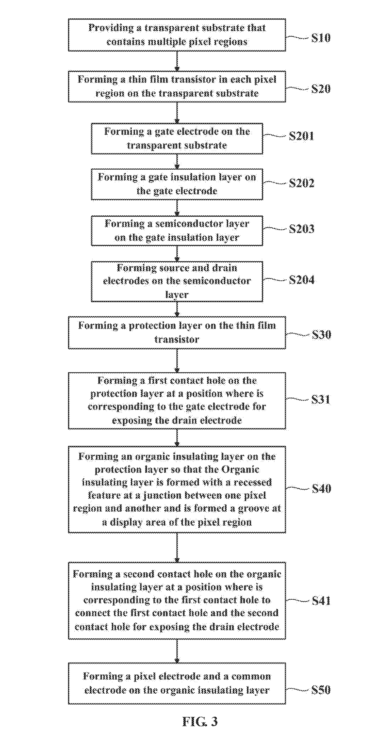
Figure 3
Abstract
Description
FIELD OF THE INVENTION
[0001] The present invention relates to a thin film transistor and a manufacturing method thereof, and more particularly, relates to a thin film transistor array substrate, manufacturing method thereof and liquid crystal panel.BACKGROUND OF THE INVENTION
[0002] Liquid crystal displays are the most widely used flat panel displays and have been widely used in various electronic equipments increasingly, such as mobile phone, personal digital assistant (PDA), digital camera, computer screen and laptop screen. With the development and progress of liquid crystal display technology, a higher requirement for display performances and designs of the liquid crystal displays has also been brought forward.
[0003] Liquid crystal panels are main accessories to the liquid crystal displays, which comprises a thin film transistor (TFT) array substrate and a color filer (CF) substrate that are vacuum laminated, and a liquid crystal layer and alignment films that are disposed between t...
Examples
Embodiment Construction
[0026]Embodiments, for purposes of explanation, are set forth in order to provide a thorough understanding of the present invention and not to limit the technical solution of the present invention. Directional terms described by the present invention, such as upper, lower, front, back, left, right, inner, outer, side, and etc., are only directions by referring to the accompanying drawings. And thus the used directional terms are used to describe and understand the present invention, but the present invention is not limited thereto. In particular, for conveniently describing, FIGS. 4A-4H are shown in simplification, wherein the number of the traces is simplified and some of details which are unrelated to the description are also omitted.
[0027]A thin film transistor array substrate 100 is provided in a preferred embodiment of the present invention, which has a transparent substrate 101 and comprises regular data lines and gate lines (not shown in the figure) that divides the transpare...