
Display panel and method of manufacturing display panel
Patent Information
- Authority / Receiving Office
- US · United States
- Current Assignee / Owner
- Publication Date
- 2021-10-28
Smart Images
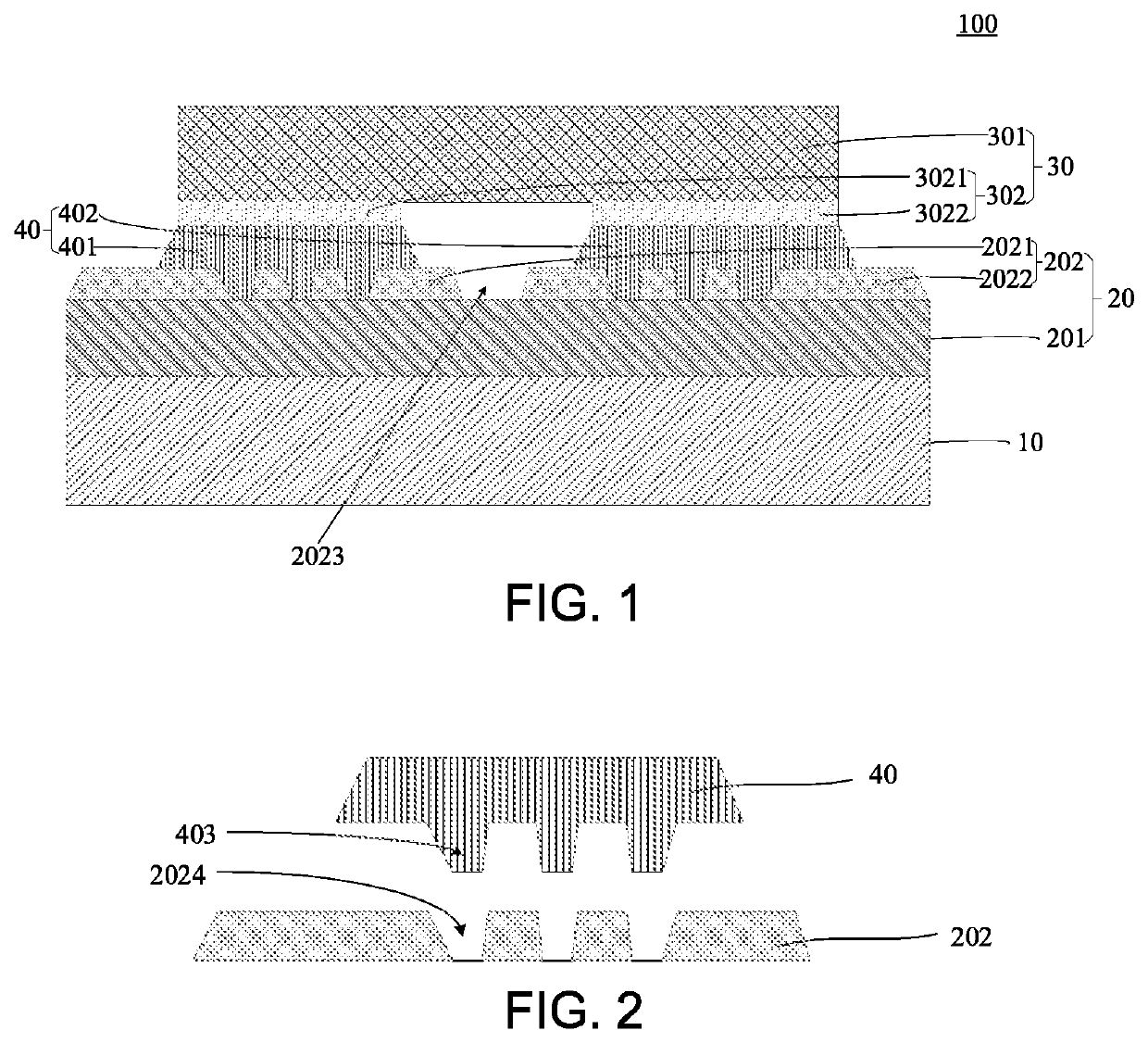
Figure 1 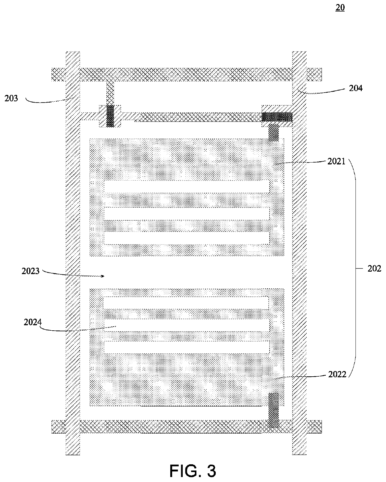
Figure 2 
Figure 3
Abstract
Description
FIELD OF INVENTION
[0001] The present disclosure relates to the field of display technologies, and more particularly to a display panel and a method of manufacturing a display panel.BACKGROUND OF INVENTION
[0002] With the development of display technologies, micro light emitting diodes (LEDs) have been gradually applied to electronic devices due to their high brightness, good luminous efficiency, and low power consumption.
[0003] However, due to special requirements of epitaxial substrates and epitaxial processes of the micro LEDs, the micro LEDs cannot be directly disposed on a thin film transistor (TFT). Therefore, after a fabrication of the micro LEDs is completed, the micro LEDs need to be electrically connected to a substrate through a bonding process.
[0004] Due to a small size of a connection portion of the micro LED, after the bonding process, the micro LED may have issues such as chip falling or virtual connection, resulting in poor soldering of the micro LED and dark spots.SUMMARY...
Examples
Embodiment Construction
[0027]The accompanying figures to be used in the description of embodiments of the present disclosure or prior art will be described in brief to more clearly illustrate the technical solutions of the embodiments or the prior art. The accompanying figures described below are only part of the embodiments of the present disclosure, from which figures those skilled in the art can derive further figures without making any inventive efforts.
[0028]An embodiment of the present disclosure provides a display panel and a method of manufacturing a display panel, which will be separately described in detail below.
[0029]Referring to FIG. 1, FIG. 1 is a schematic structural view of a display panel according to an embodiment of the present disclosure. In a display panel 100 of an embodiment of the present disclosure, the display panel 100 includes a substrate layer 10, a thin film transistor layer 20, a light emitting device 30, and a soldering portion 40.
[0030]Material of the substrate layer 10 ma...