
Array substrate and display panel
Patent Information
- Authority / Receiving Office
- US · United States
- Current Assignee / Owner
- Publication Date
- 2019-03-28
Smart Images
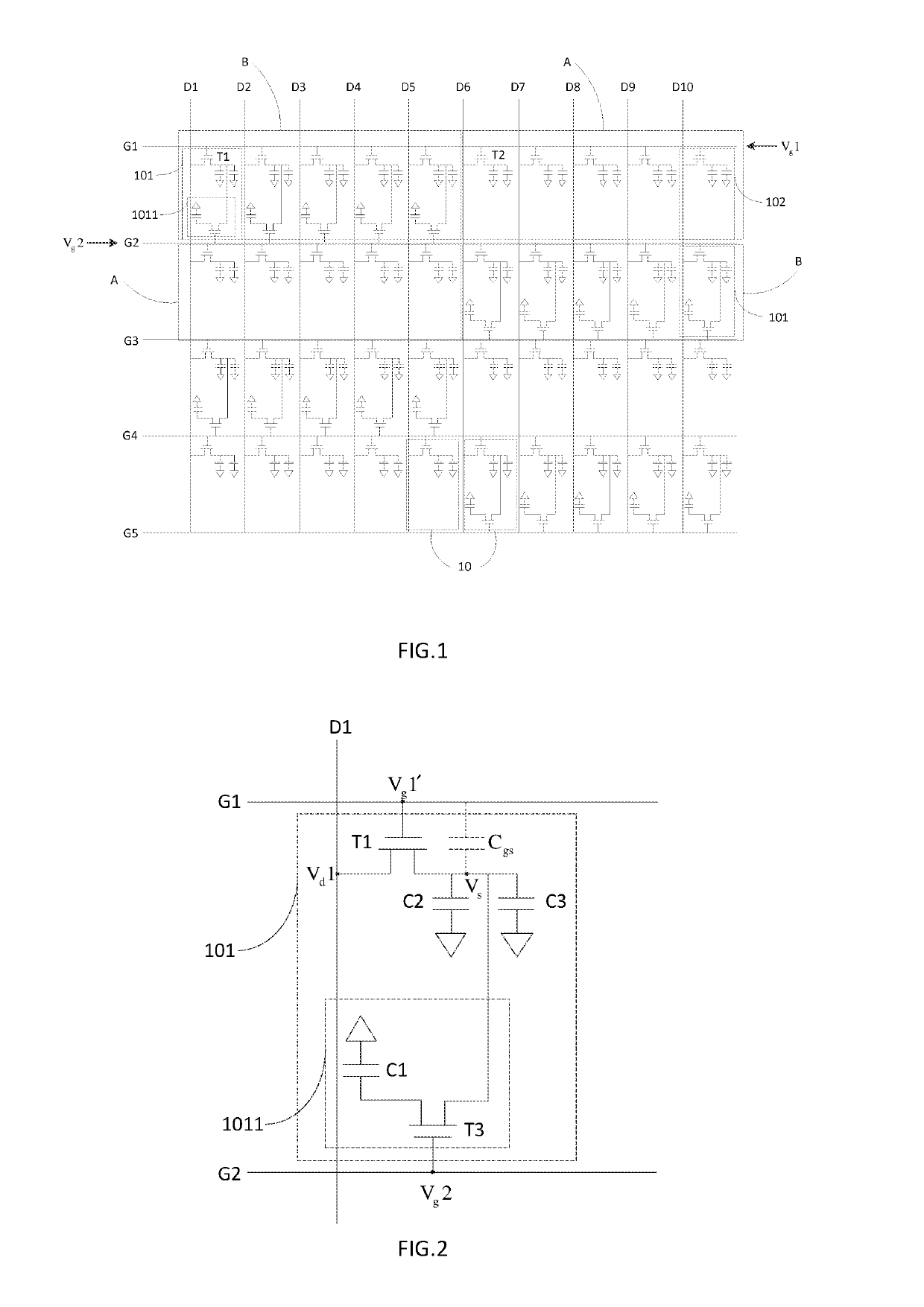
Figure 1 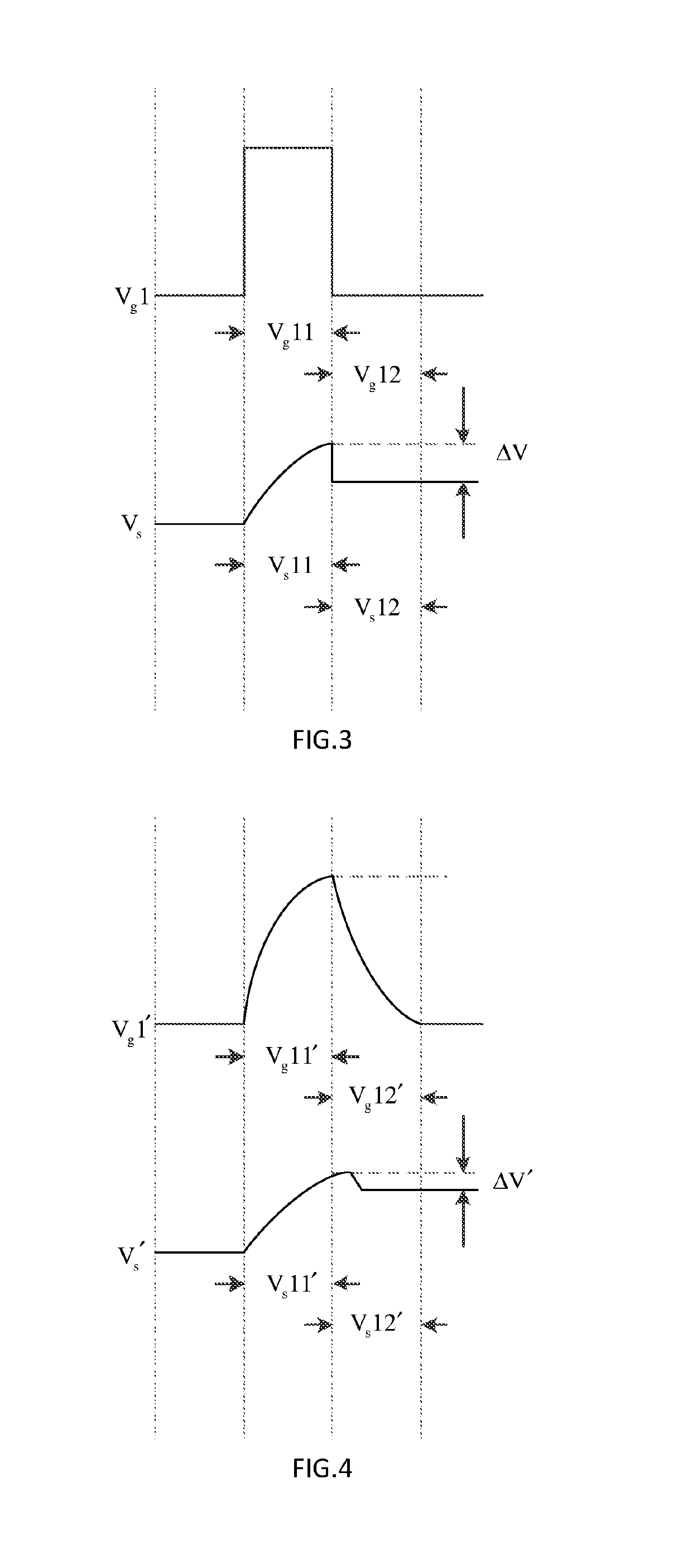
Figure 2 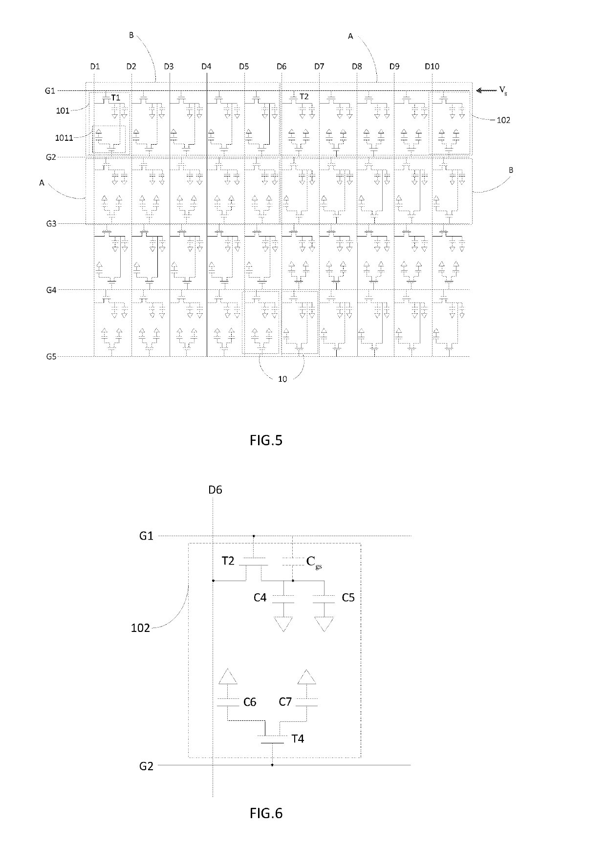
Figure 3
Abstract
Description
BACKGROUND1. Technical Field
[0001] The present disclosure relates to a display field, and more particularly to an array substrate and a display panel.2. Description of Related Art
[0002] The thin film transistor (TFT) adopted in display devices mainly includes amorphous silicon TFTs and poly-silicon TFTs. With the increasing of the using time, mobility and photosensitivity of the amorphous silicon TFTs may be largely reduced. However, the low temperature poly-silicon (LTPS) may have better mobility and stability when comparing with the amorphous silicon.
[0003] The gate driver on array (GOA) of the LTPS panels usually adopts the one-way driving interlaced scanning mode. That is, the gate drivers are configured on both sides of the LTPS panel, and the gate drivers may be turned on according to the scanning timings of the scanning lines. However, the signals may have time difference between the starting end and the terminal end of the scanning line due to the time-delay of the resistor and...
Examples
Embodiment Construction
[0014]To clarify the purpose, technical solutions, and the advantages of the disclosure, embodiments of the invention will now be described more fully hereinafter with reference to the accompanying drawings.
[0015]Referring to FIG. 1, the present disclosure relates to an array substrate, including: a plurality of scanning lines Gn (for example G1, G2, G3, G4 and G5 in the present embodiment), a plurality of data lines Dn (for example D1, D2, D3, D4, D5, D6, D7, D8, D9 and D10 in the present embodiment). The data lines Dn and the scanning lines Gn respectively intersect with each other to form a plurality of pixel cells 10.
[0016]The pixel cells 10 may be divided into the pixel cells within a first area (A) and the pixel cells within a second area (B) along a direction of the scanning lines Gn. A distance between the first area (A) and an input end of scanning signals is less than a distance between the second area (B) and the input end of the scanning signals. Each of the pixel cells ...