
Semiconductor package and manufacturing method thereof
a technology of semiconductor and packaging, applied in the direction of semiconductor/solid-state device details, electrical apparatus, semiconductor devices, etc., can solve the problem of miniaturization of semiconductor packages, achieve the effect of reducing fabrication costs and packaging volume, improving efficiency, and reducing signal transmission path
Patent Information
- Authority / Receiving Office
- US · United States
- Patent Type
- Applications(United States)
- Current Assignee / Owner
- Publication Date
- 2019-07-11
Smart Images
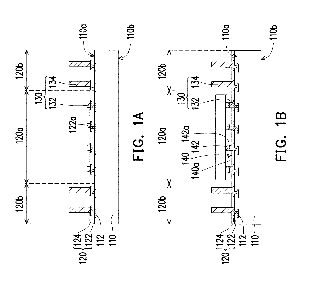
Figure 1 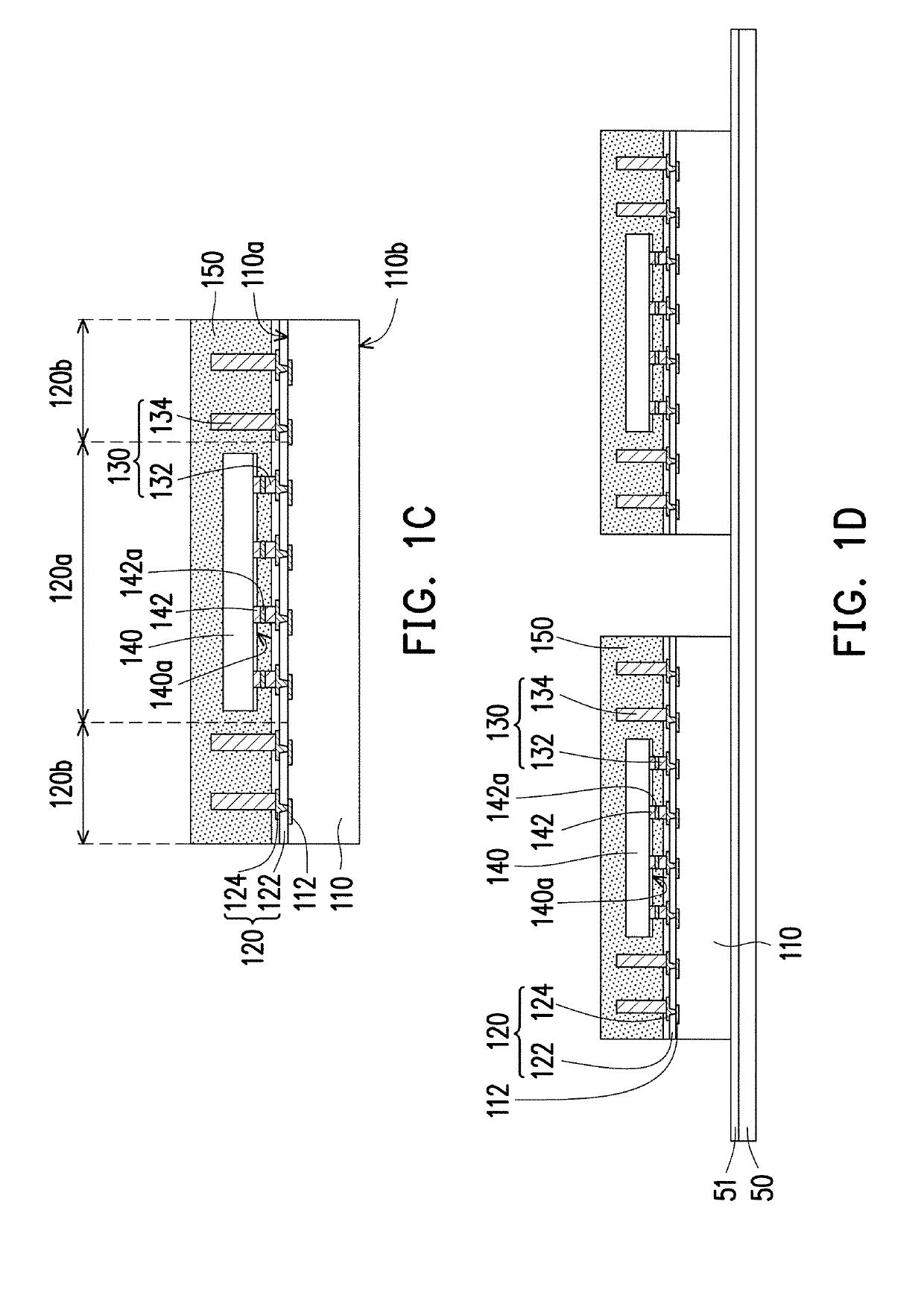
Figure 2 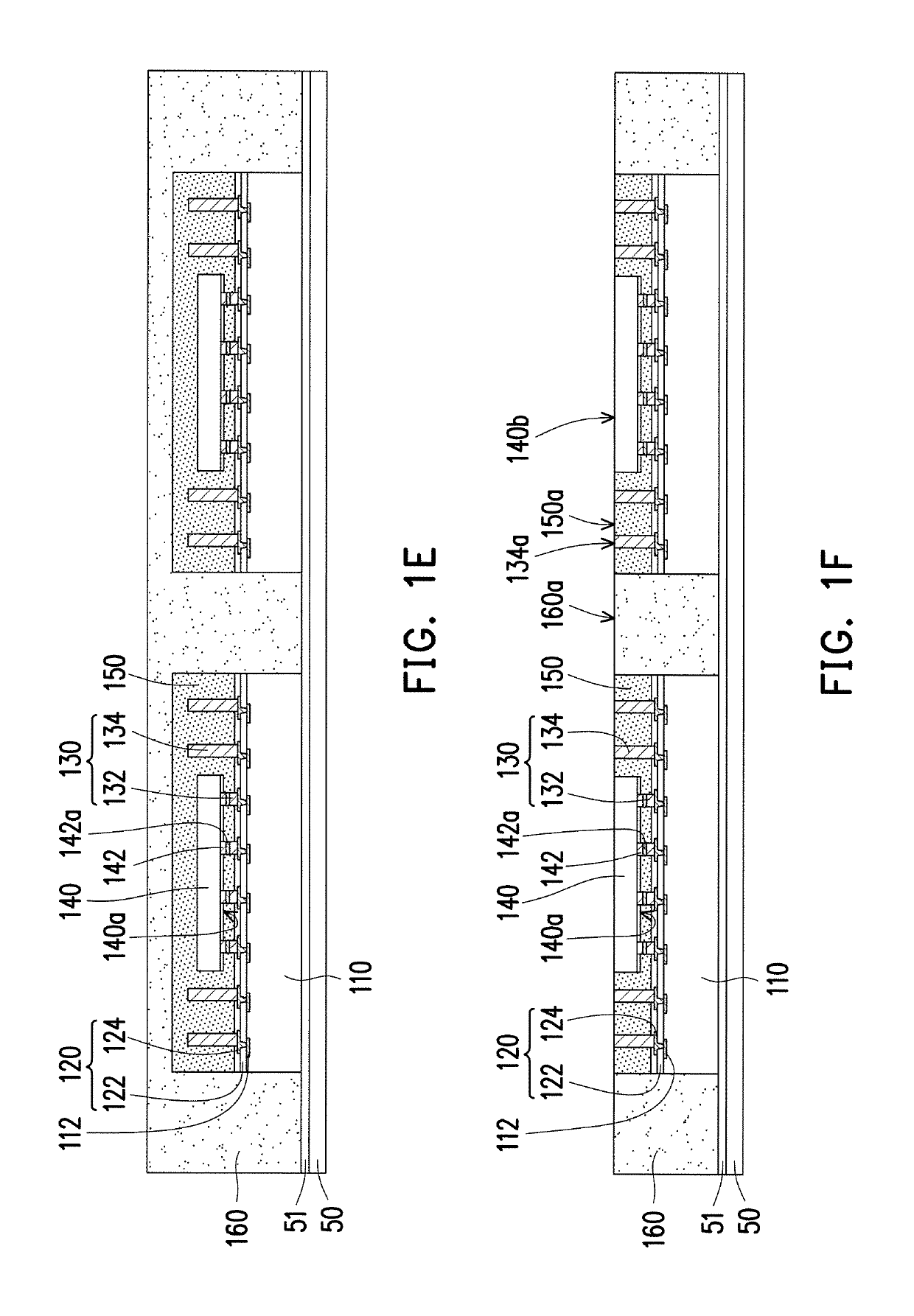
Figure 3
Abstract
Description
BACKGROUND OF THE INVENTION1. Field of the Invention
[0001] The present invention generally relates to a package structure and a manufacturing method thereof; and more particularly, to a semiconductor package and a manufacturing method thereof.2. Description of Related Art
[0002] In recently years, electronic apparatus are more important for human's life. In order for electronic apparatus design to achieve being light, slim, short, and small, semiconductor packaging technology has kept progressing, in attempt to develop products that are smaller in volume, lighter in weight, higher in integration, and more competitive in market. Since the chip package technique is highly influenced by the development of integrated circuits, therefore, as the size of electronics has become demanding, so does the package technique. As such, miniaturizing the semiconductor package while maintaining the process simplicity has become a challenge to researchers in the field.SUMMARY OF THE INVENTION
[0003] The d...
Examples
Embodiment Construction
[0014]Reference will now be made in detail to the present preferred embodiments of the invention, examples of which are illustrated in the accompanying drawings. Wherever possible, the same reference numbers are used in the drawings and the description to refer to the same or like parts.
[0015]FIG. 1A to FIG. 1I are schematic cross-sectional views illustrating a manufacturing method of a semiconductor package according to an embodiment of the disclosure. A wafer including a plurality of first semiconductor dies 110 arranged in an array may be provided. It should be noted that for simplicity of illustration, single first semiconductor die 110 is shown in FIG. 1A to FIG. 1C, but the invention is not limited to. Referring to FIG. 1A, the first semiconductor die 110 may include a first active surface 110a, a first back surface 110b opposite to the first active surface 110a, and a plurality of conductive pads 112 on the first active surface 110a. In some embodiments, the first semiconduct...