
Ion implant dose control
a technology of ion implants and substrates, applied in the direction of irradiation devices, table equipments, nuclear engineering, etc., can solve the problems of high beam current measurement errors, time-consuming and expensive failure to achieve such standards, and achieve the effect of optimising pump down time and eliminating quadrature variation
Patent Information
- Authority / Receiving Office
- US · United States
- Patent Type
- Patents(United States)
- Current Assignee / Owner
- Publication Date
- 2005-03-22
- Estimated Expiration
- Not applicable · inactive patent
Smart Images
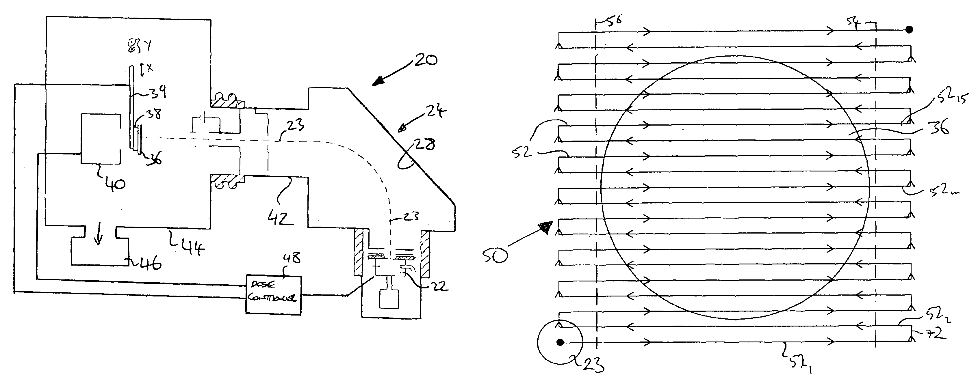
Figure 1 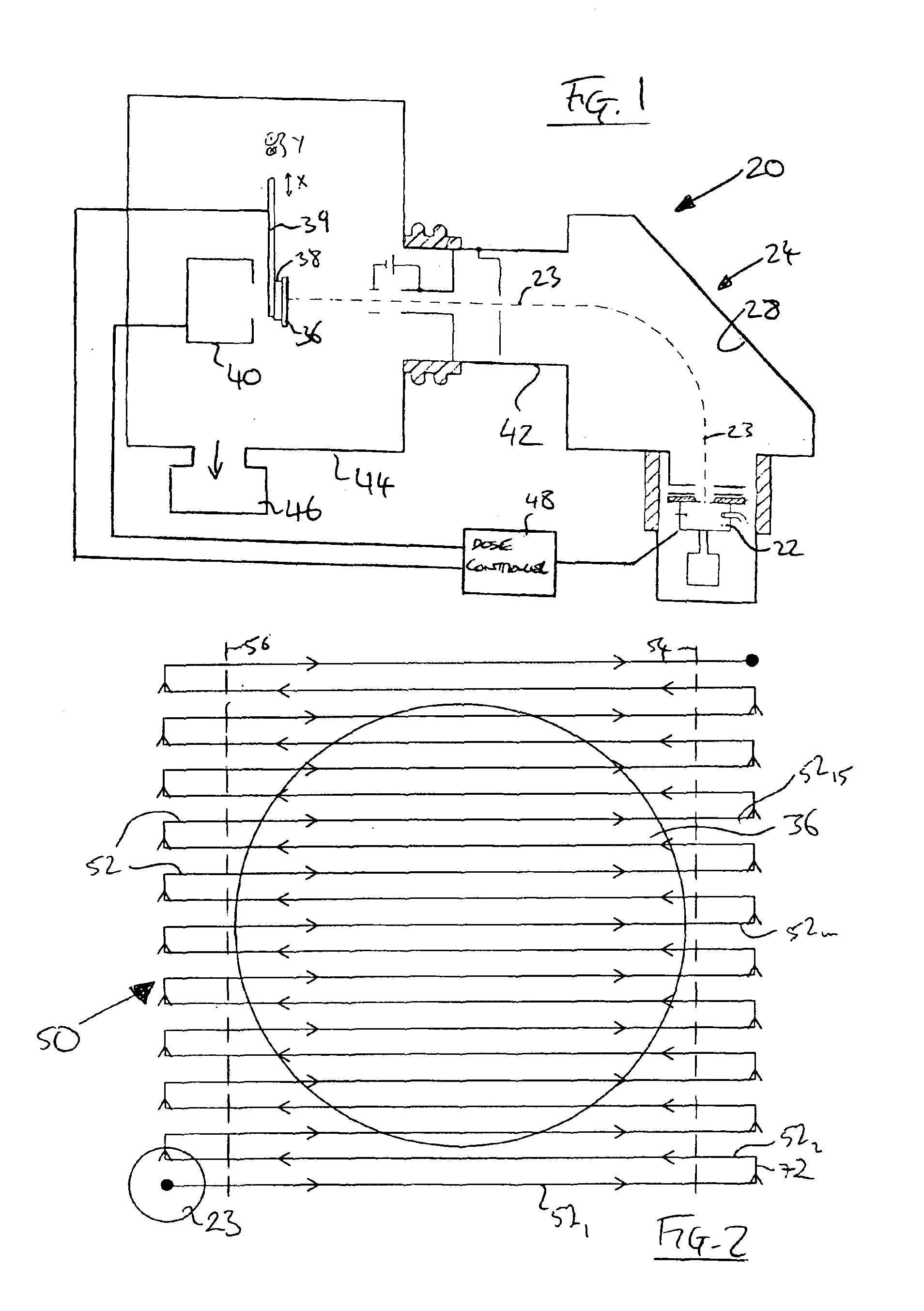
Figure 2 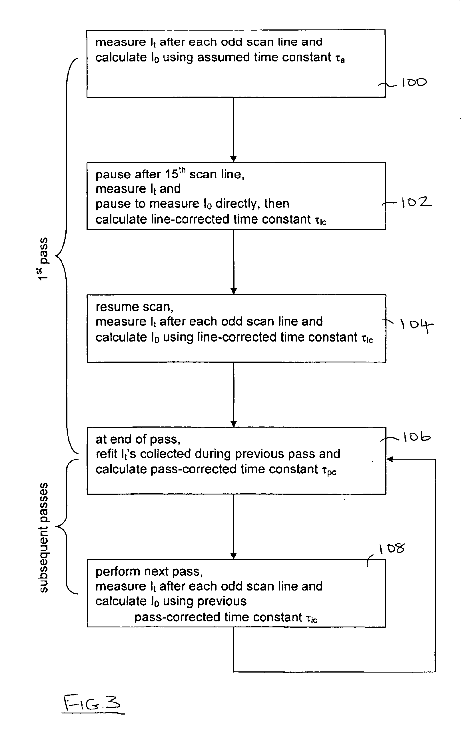
Figure 3
Abstract
Description
FIELD OF THE INVENTIONThis invention is concerned with improvements in or relating to the control of ion dosing a substrate, such as doping semiconductor wafers.BACKGROUND OF THE INVENTIONIon implanters are commonly used in the manufacture of semiconductor products for implanting ions into semiconductor substrates to change the conductivity of the material in such substrates or in pre-defined regions thereof. Ion implanters generally comprise an ion source for generating a beam of ions, a mass analyser for selecting a particular species of ions from the ion beam and means to direct the mass-selected ion beam through a vacuum chamber onto a target substrate supported on a substrate holder.Most frequently, the ion beam cross-sectional area at the target substrate is less that the surface area of the substrate which necessitates scanning of the beam over the substrate using a one or two-dimensional scan so that the beam covers the whole surface of the substrate. Three scanning techniqu...
Examples
Embodiment Construction
The present invention can readily be illustrated with reference to such a single wafer implant machine, such as the ion implanter 20 shown in FIG. 1. However, it should be understood that the invention may also be embodied in batch implanters of the type in which a batch of wafers mounted on a spinning wheel is processed simultaneously.
The single wafer machine of FIG. 1 comprises an ion source 22, such as a Freeman or Bernas ion source, that is supplied with a pre-cursor gas for producing an ion beam 23 to be implanted into a wafer 36. The ions generated in the ion source 22 are extracted by an extraction electrode assembly into a flight tube 24 that includes a mass-analysis arrangement 28 comprising a mass-analysing magnet and a mass-resolving slit, as is well known in the art. Upon entering the mass-analysis arrangement 28 within the flight tube 24, the electrically charged ions are deflected by the magnetic field of the mass-analysis magnet. The radius and curvature of each ion's...