
Process for improving dielectric properties in low-k organosilicate dielectric material
a dielectric material and organosilicate technology, applied in the field of semiconductor/solid-state device manufacturing, electrical equipment, basic electric elements, etc., can solve the problems of increasing both leakage current and dielectric constant, interconnect delay becomes a significant performance barrier for high-speed signal conduction, and material damage is believed to occur, etc., to achieve short treatment time, improve efficiency, and reduce pressure
Patent Information
- Authority / Receiving Office
- US · United States
- Patent Type
- Patents(United States)
- Current Assignee / Owner
- Publication Date
- 2006-07-11
- Estimated Expiration
- Not applicable · inactive patent
Smart Images
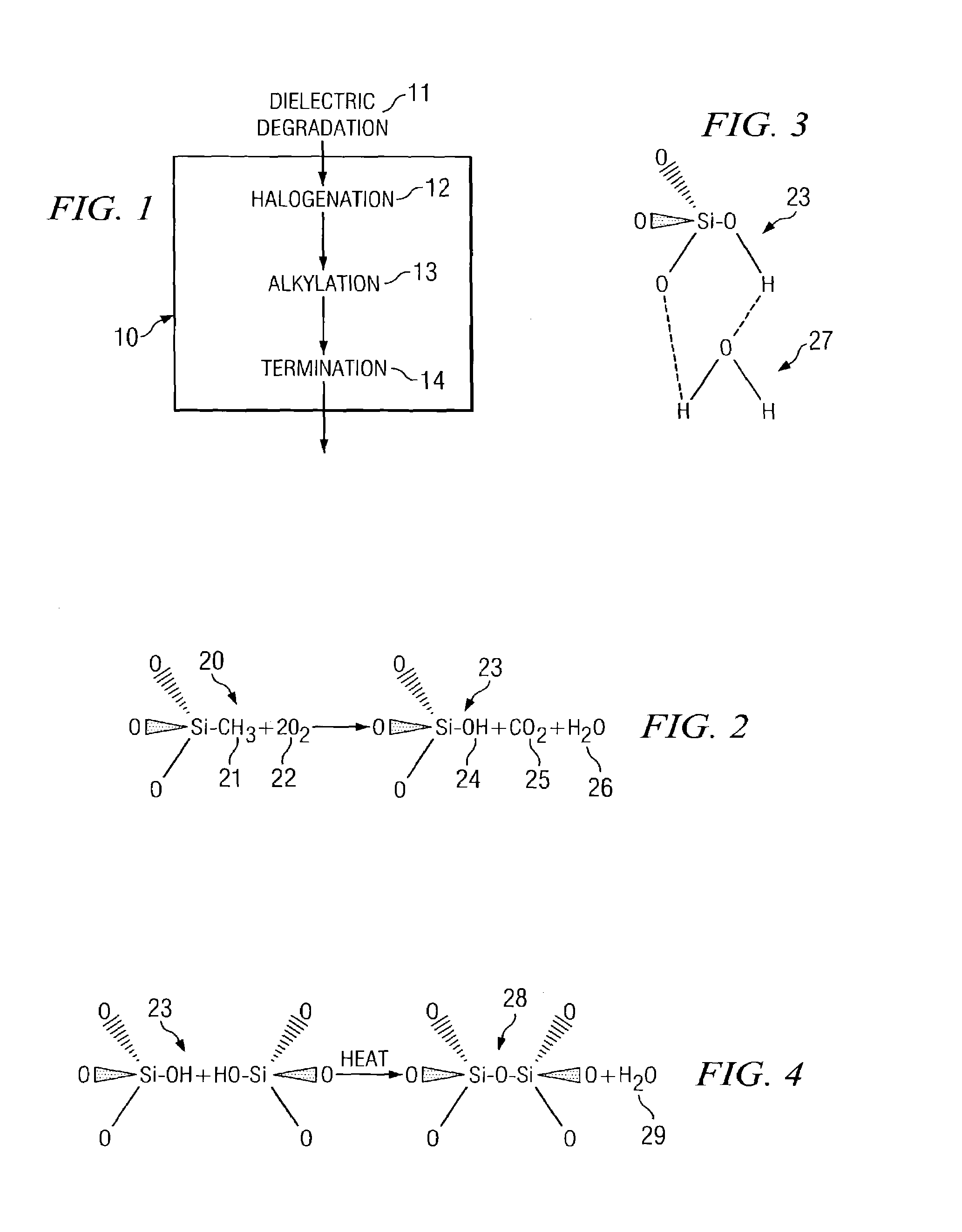
Figure 1 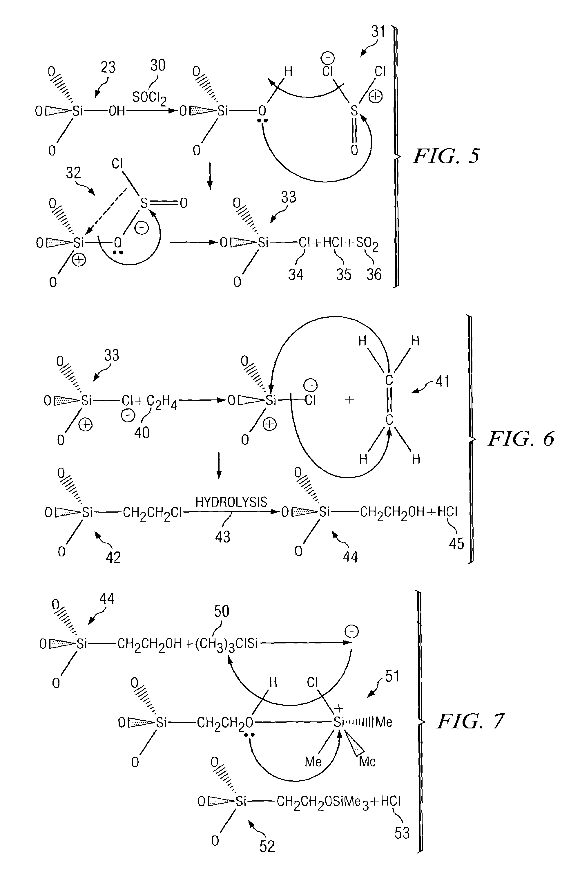
Figure 2
Abstract
Description
TECHNICAL FIELD
[0001] The present invention relates generally to semiconductor fabrication processes and more particularly to a process for repairing degradation of dielectric properties of low-k organosilicate dielectric material.BACKGROUND
[0002] As semiconductor devices are scaled down to smaller feature sizes, interconnect delay becomes a significant performance barrier for high-speed signal conduction. The use of dielectric materials with a lower dielectric constant (k) can significantly improve performance measures by reducing signal propagation time delay, cross talk, and power consumption in semiconductor devices having a multilevel interconnect architecture. The most-used dielectric material for semiconductor fabrication has been silicon oxide (SiO2), which has a dielectric constant in the range of k=3.9 to 4.5, depending on its method of formation. Dielectric materials with k less than 3.9 are classified as ‘low-k dielectrics’. Some low-k dielectrics are organosilicates forme...
Examples
Embodiment Construction
[0023]The making and using of the presently preferred embodiments are discussed in detail below. It should be appreciated, however, that the present invention provides many applicable inventive concepts that can be embodied in a wide variety of specific contexts. The specific embodiments discussed are merely illustrative of specific ways to make and use the invention, and do not limit the scope of the invention.
[0024]The present invention will be described with respect to preferred embodiments in a specific context, namely an organosilicate low-k dielectric whose dielectric properties have been degraded through oxidation by exposure to O2 plasma. The invention may also be applied, however, to such dielectrics that have had silicon-carbon bonds broken by other steps in the semiconductor fabrication process.
[0025]With reference now to FIG. 1, there is shown a process 10 embodying the present invention. A previous step in the semiconductor fabrication process 11, degrades the dielectri...