
Method and structure for a self-aligned silicided word line and polysilicon plug during the formation of a semiconductor device
a technology of polysilicon plug and silicon silicide, which is applied in the direction of semiconductor devices, basic electric elements, electrical equipment, etc., can solve the problems of increasing junction leakage, increasing increasing the difficulty of scaling titanium silicide, so as to reduce the size of features, reduce the difficulty of scaling, and reduce the effect of problems
Patent Information
- Authority / Receiving Office
- US · United States
- Patent Type
- Patents(United States)
- Current Assignee / Owner
- Publication Date
- 2006-10-10
Smart Images
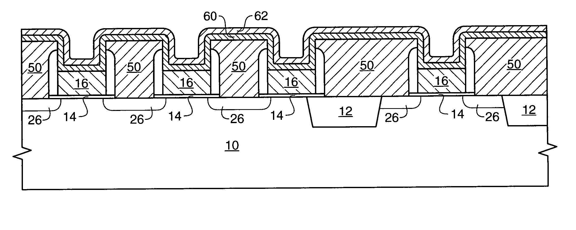
Figure 1 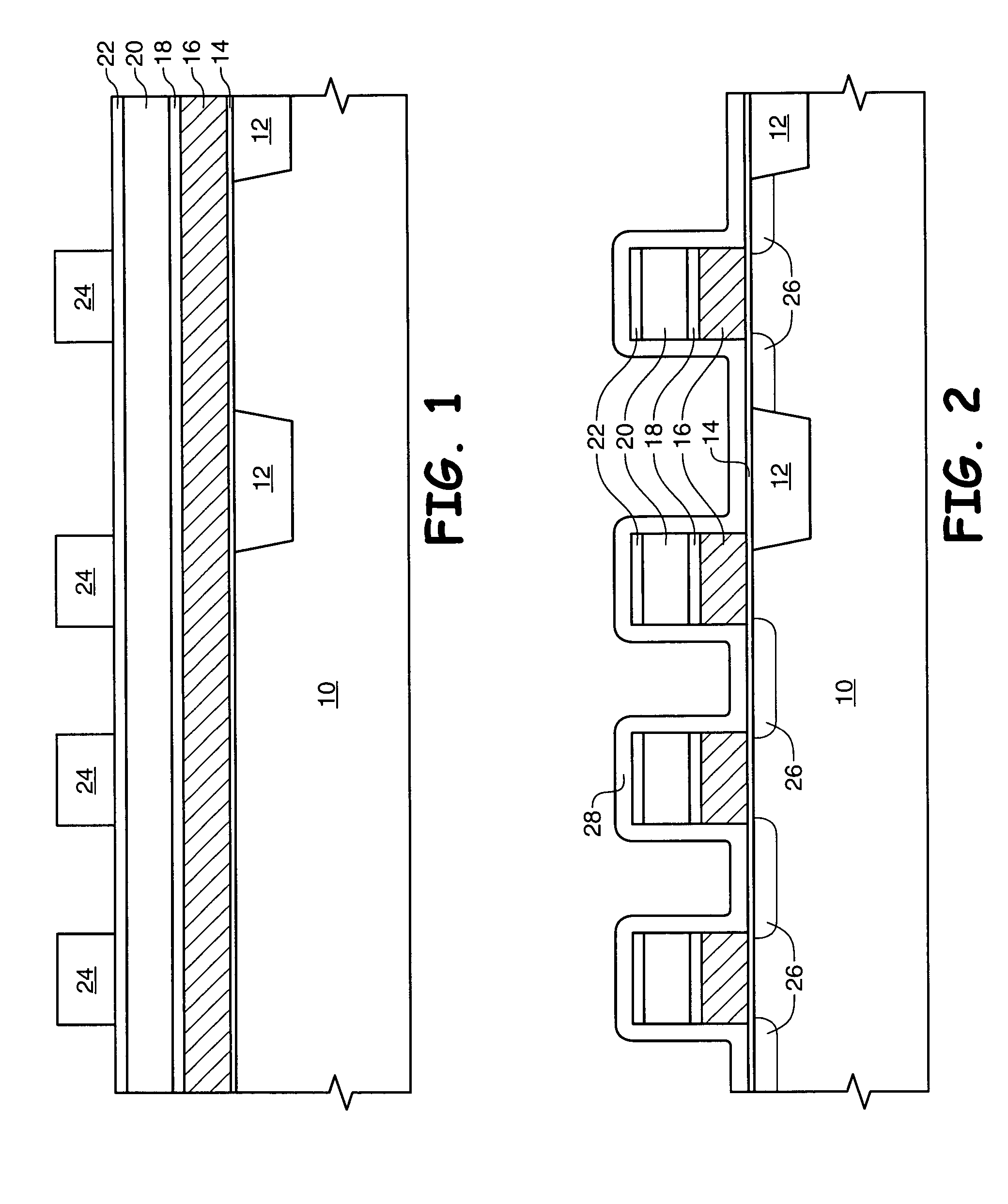
Figure 2 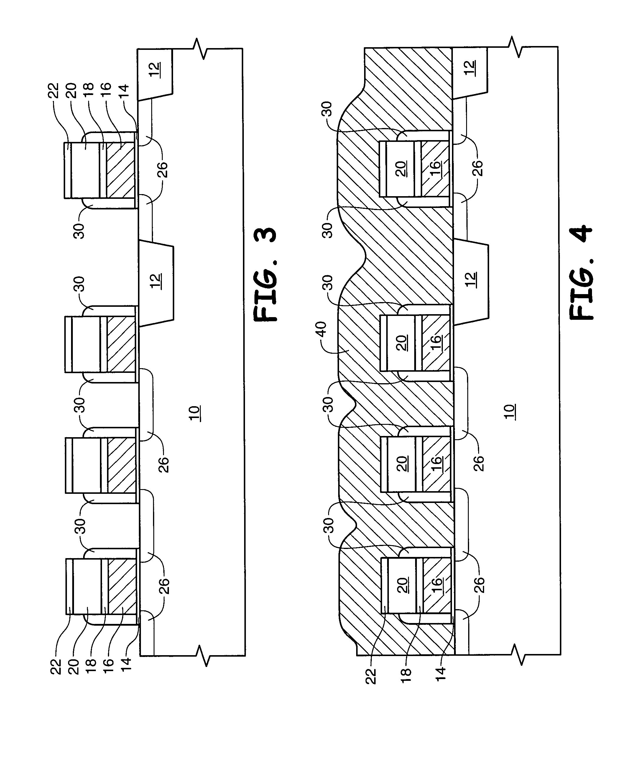
Figure 3
Abstract
Description
FIELD OF THE INVENTION
[0001] This invention relates to the field of semiconductor manufacture, and more particularly to a process for forming self-aligned conductive structures having enhanced conductivity through an enhancement layer, and an inventive structure resulting from the process.BACKGROUND OF THE INVENTION
[0002] Structures such as polycrystalline silicon (polysilicon) plugs, interconnects, and transistor gates are commonly formed during the manufacture of semiconductor devices such as microprocessors, memory devices, and logic devices. To manufacture a plug, for example, a masked dielectric layer is formed over an underlying substrate assembly and an etch is completed to form a hole in the dielectric which exposes the underlying structure in the area where contact is to be made. A blanket polysilicon layer is deposited over the dielectric layer which fills the hole in the dielectric layer and contacts the underlying structure. The polysilicon is then removed from a planar su...
Examples
Embodiment Construction
[0017]The term “wafer” is to be understood as a semiconductor-based material including silicon, silicon-on-insulator (SOI) or silicon-on-sapphire (SOS) technology, doped and undoped semiconductors, epitaxial layers of silicon supported by a base semiconductor foundation, and other semiconductor structures. Furthermore, when reference is made to a “wafer” in the following description, previous process steps may have been performed to provide regions or junctions in or over the base semiconductor structure or foundation. Additionally, when reference is made to a “substrate assembly” in the following description, the substrate assembly may include a wafer with layers including dielectrics and conductors, and features such as transistors, formed thereover, depending on the particular stage of processing. In addition, the semiconductor need not be silicon-based, but could be based on silicon-germanium, silicon-on-insulator, silicon-on-sapphire, germanium, or gallium arsenide, among other...