
Optoelectronic devices and methods of production
Patent Information
- Authority / Receiving Office
- US · United States
- Current Assignee / Owner
- Publication Date
- 2006-12-19
- Estimated Expiration
- Not applicable · inactive patent
Smart Images
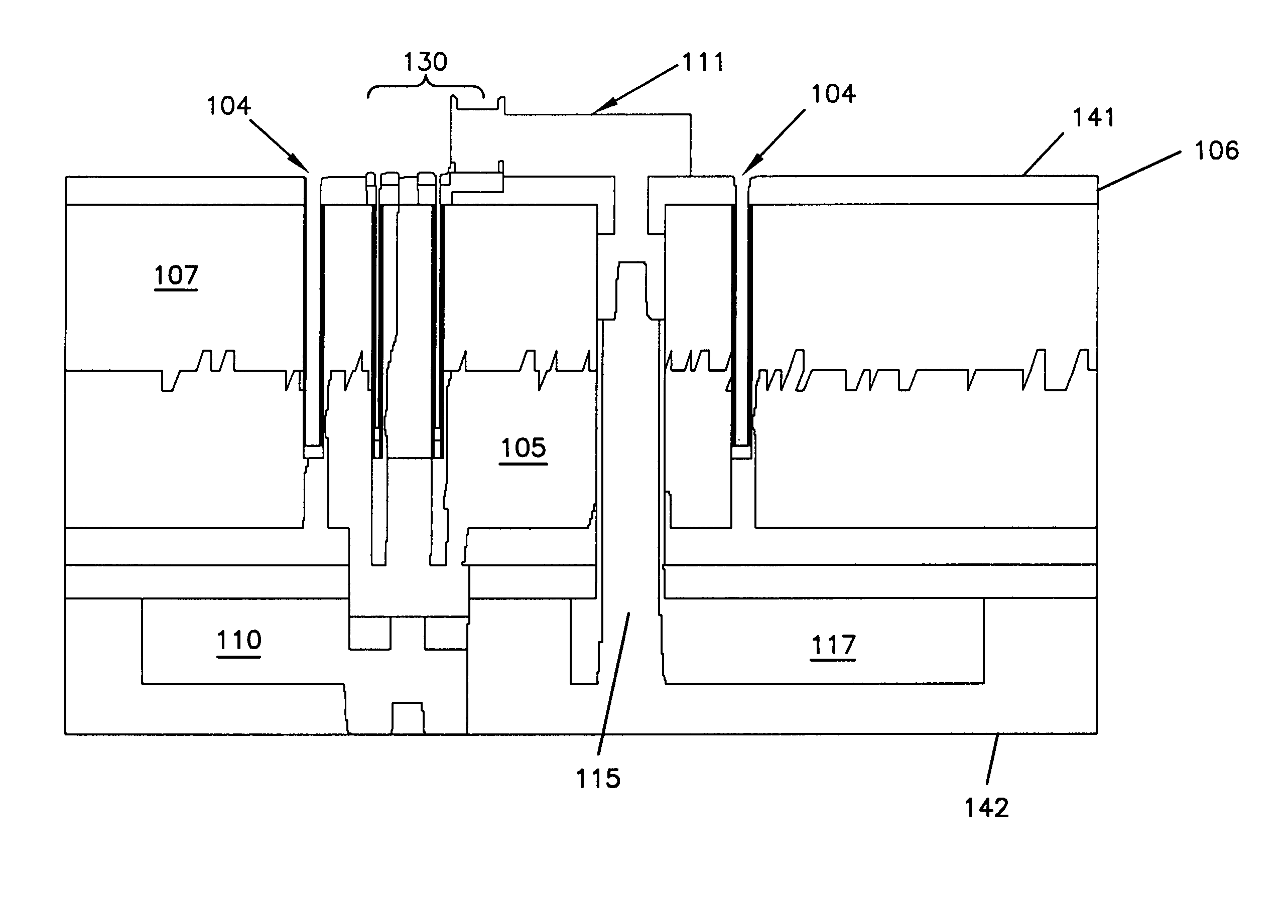
Figure 1 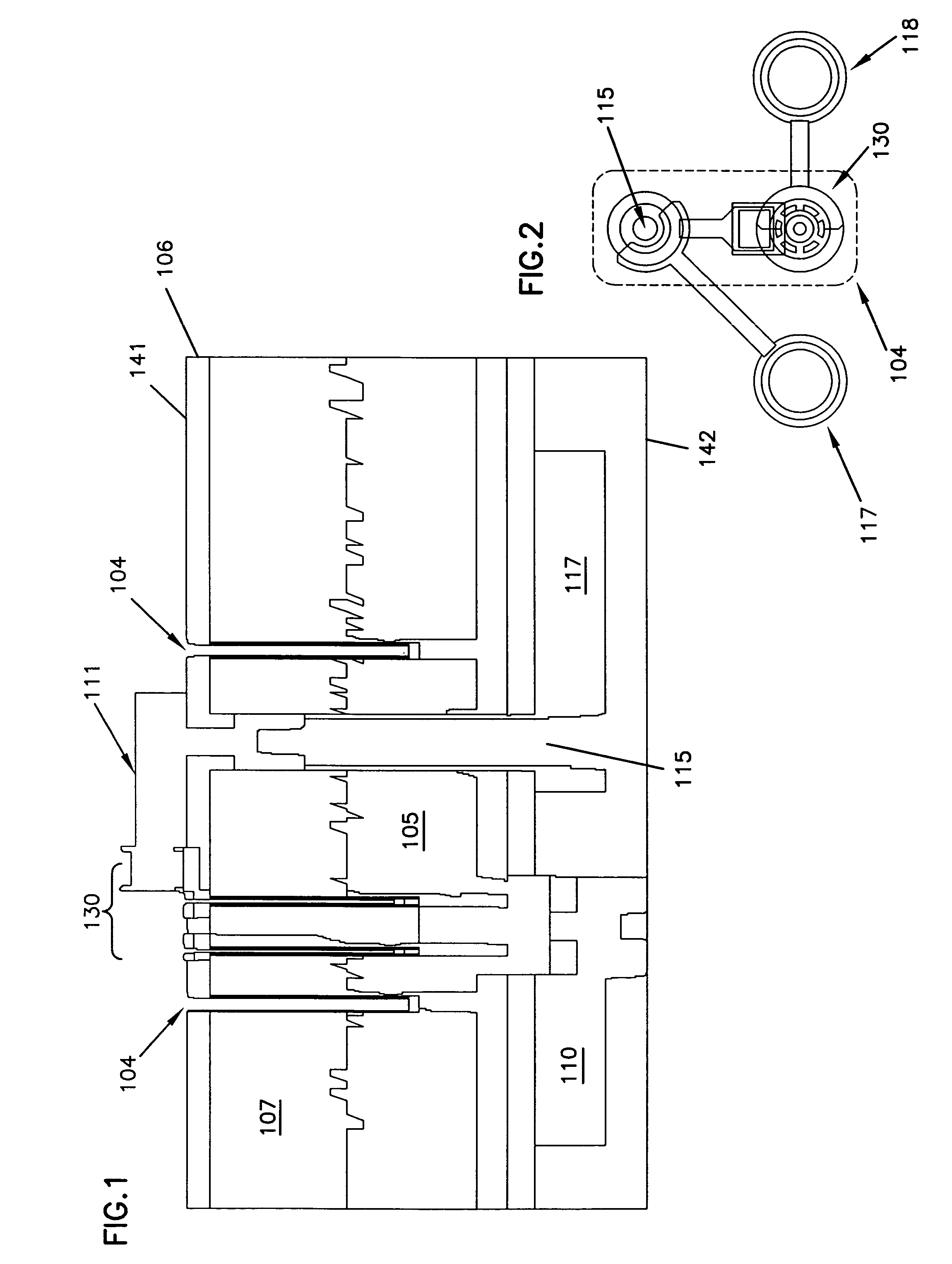
Figure 2 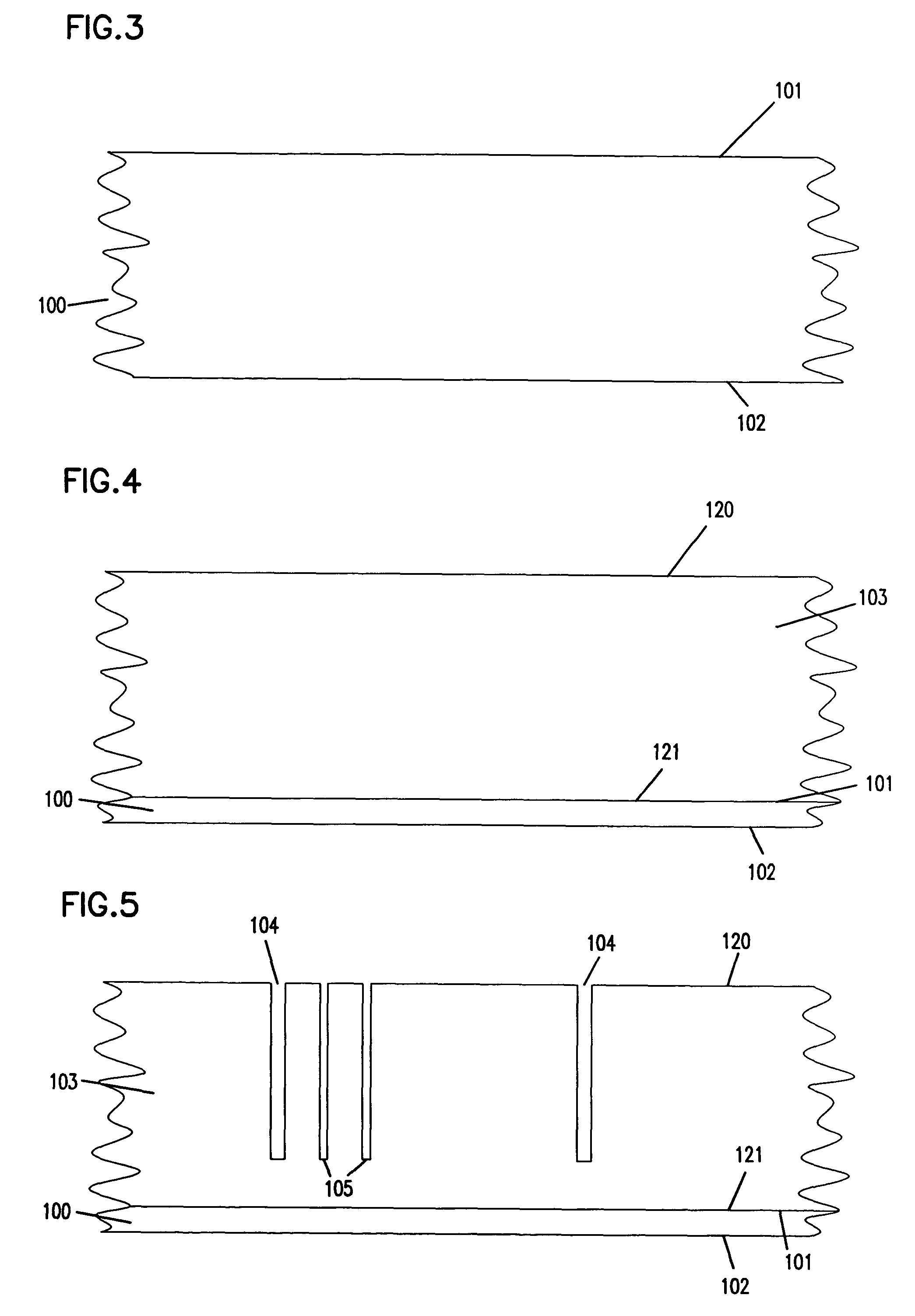
Figure 3
Abstract
Description
[0001] This application is a divisional of application Ser. No. 10 / 037,013, filed Dec. 31, 2001, now U.S. Pat. No. 6,724,798 which application(s) are incorporated herein by reference.UNITED STATES GOVERNMENT RIGHTS
[0002] This invention was made with the United States Government support under 70NAHB8H4023 awarded by National Institute of Standards and Technology (NIST).FIELD OF THE INVENTION
[0003] The invention generally pertains to a novel production method and the resulting optoelectronic devices. More particularly, the invention pertains to a novel method of producing optoelectronic devices, such as vertical cavity surface emitting lasers (VCSELs) and providing isolated contacts for these devices, enabling their use in high speed, low cost multi-device arrays.BACKGROUND OF THE INVENTION
[0004] Smart pixel arrays (SPAs) are devices containing arrays of vertical cavity surface emitting lasers (VCSELs) and photodetectors. SPAs are capable of performing high-speed switching and routing of ...
Examples
Embodiment Construction
[0020]The invention includes devices and methods of producing the same with at least an optoelectronic structure, isolation moat, and through wafer via. The method of the invention includes producing an optoelectronic structure, forming a through wafer via and forming an isolation moat.
The Device
[0021]FIGS. 1 and 2 are sectional views, and it should therefore be appreciated that the illustrations depicted in FIGS. 1 and 2 can extend into and out of the drawings, thereby allowing for the depiction of arrays of the various structures.
[0022]FIG. 1 illustrates a device in accordance with one aspect of the invention. FIG. 1 is a cross sectional view of such an exemplary device. FIG. 2 also illustrates a device in accordance with one aspect of the invention. FIG. 2 is a top view of such an exemplary device showing the spatial layout of the structures given therein. As seen in FIGS. 1 and 2, a device in accordance with the invention comprises an optoelectronic structure 130, an isolation m...