
Composition for forming porous film, porous film and method for forming the same, interlevel insulator film, and semiconductor device
Patent Information
- Authority / Receiving Office
- US · United States
- Current Assignee / Owner
- Publication Date
- 2007-08-02
- Estimated Expiration
- Not applicable · inactive patent
Smart Images
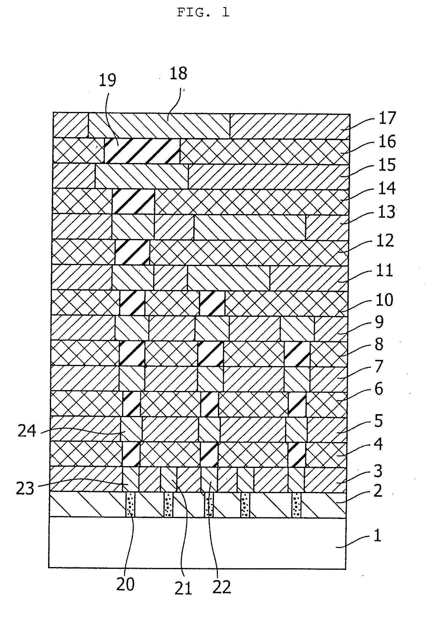
Figure 1 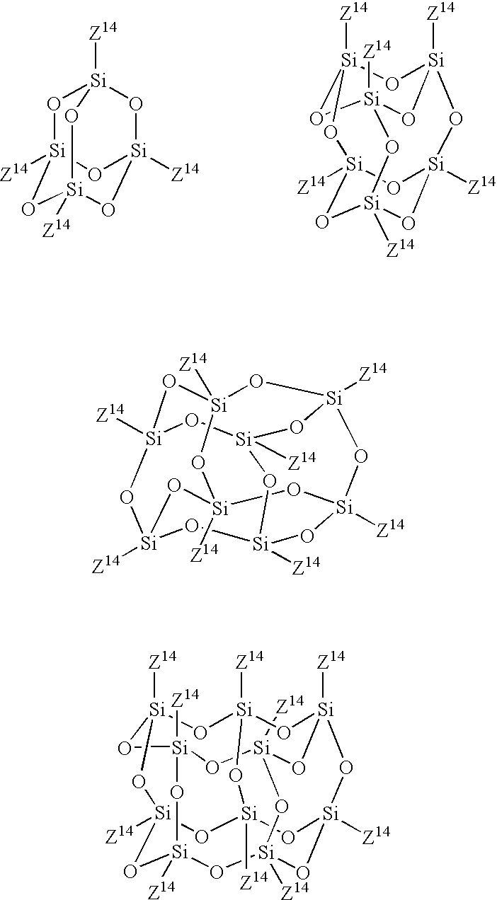
Figure 2 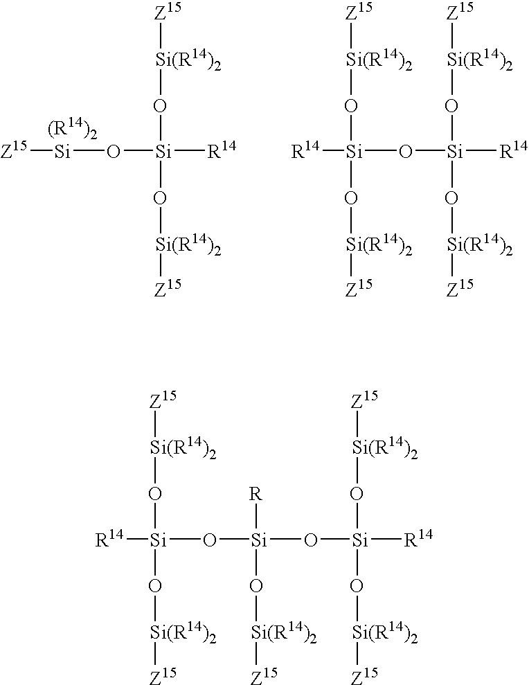
Figure 3
Abstract
Description
CROSS-REFERENCE TO RELATED APPLICATION
[0001] The present application claims priority to Japanese Patent Application No. 2002-329127, filed Nov. 13, 2002, the disclosure of which is incorporated herein by reference in its entirely. BACKGROUND OF THE INVENTION
[0002] 1. Field of the Invention
[0003] The present invention relates to a composition for film formation, which can be formed into a porous film that excels in dielectric properties, adhesion, film consistency and mechanical strength, and has reduced absorption; a porous film and a method for forming the same; and a semiconductor device, which contains the porous film inside.
[0004] 2. Description of the Related Art
[0005] In the fabrication of semiconductor integrated circuits, as the circuits are packed tighter, an increase in interconnection capacitance, which is a parasitic capacitance between metal interconnections, leads to an increase in interconnection delay time, thereby hindering the enhancement of the performance of...
Examples
synthetic examples 1 to 6
[0085] The 3.33 g of tetramethoxysilane and 2.50 g of methyltrimethylsilane, 100 ml of ethanol solvent, 53.3 g of pure water and 0.83 g of 25% ammonia water were placed in a 300 ml flask and were mixed for 3 hours at 60° C. Then, 0.25 g of cross-linking agent shown in Table 1 and 33 g of0 propylene glycol propyl ether were added thereto and the reaction was continure for further 1 hour. Next, the ethanol solvent, methanol generated by hydrolysis and water were evaporated under reduced pressure of 5.3 kPa at 60° C. to obtain residue. Propylene glycol propyl ether (PnP) was then appropriately added to the residue so that a solution of NV8% was obtained. The NV8% means a-concentration of 8% based on the calculated conversion to silica after the sintering at 400° C. for 1 hour.
TABLE 1hydrolyzableSyn.silicon compoundcross-linking agentammoniaEx.Si(OMe)4MeSi(OMe)3LS-8680*H4TH-8MH3TMH4QSiloxane-AwaterPnP**No.(g)(g)(g)(g)(g)(g)(g)(g)(g)(g)13.332.500.250.8333.323.332.500.250.8333.333.332.5...
examples 1 to 7
[0087] Using the composition described in Synthetic Examples and Table 1, spin-coating was performed on a silicon wafer. It was pre-baked at 120° C. for 2 minutes to remove the solvent and further heated at 230° C. for 3 minutes. Then, it was heated at 425° C. for 1 hour under a nitrogen gas stream so that it was matured.
[0088] The obtained film was evaluated. The film thickness was measured with an ellipsometer and the dielectric constant was measured with mercury probe 495 CV system (Japan SSM, Solid State Mesurements Corporation). The hardness and the modulus were measured with nano-indentor SA2 (Toyo Technica, MTS Corporation). The results are shown in Table 2.