
Light emitting device with a micro-reflection structure carrier
Patent Information
- Authority / Receiving Office
- US · United States
- Current Assignee / Owner
- Publication Date
- 2006-12-26
- Estimated Expiration
- Not applicable · inactive patent
Smart Images
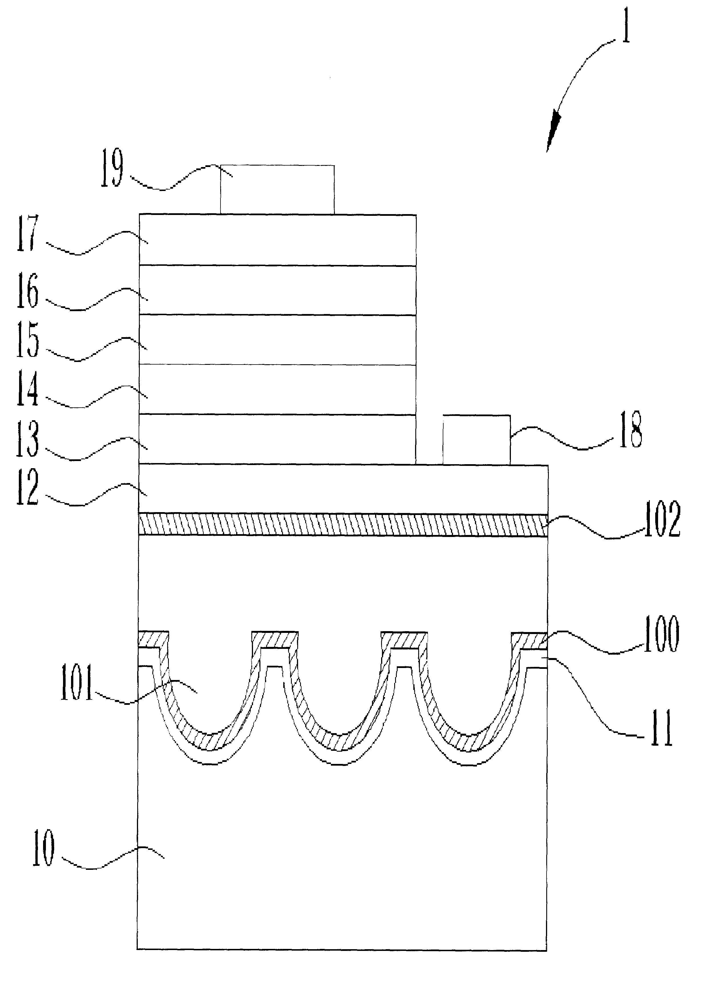
Figure 1 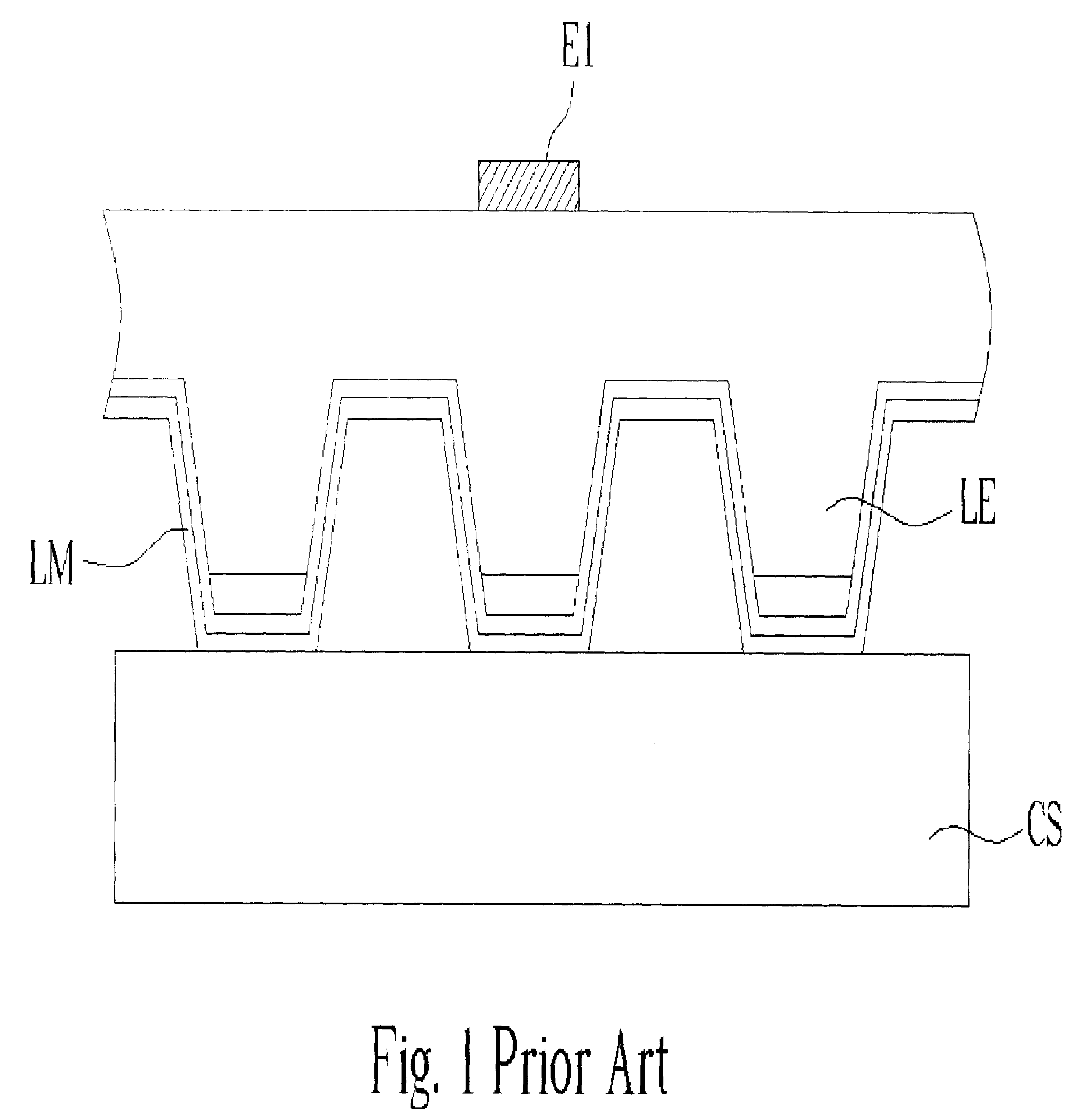
Figure 2 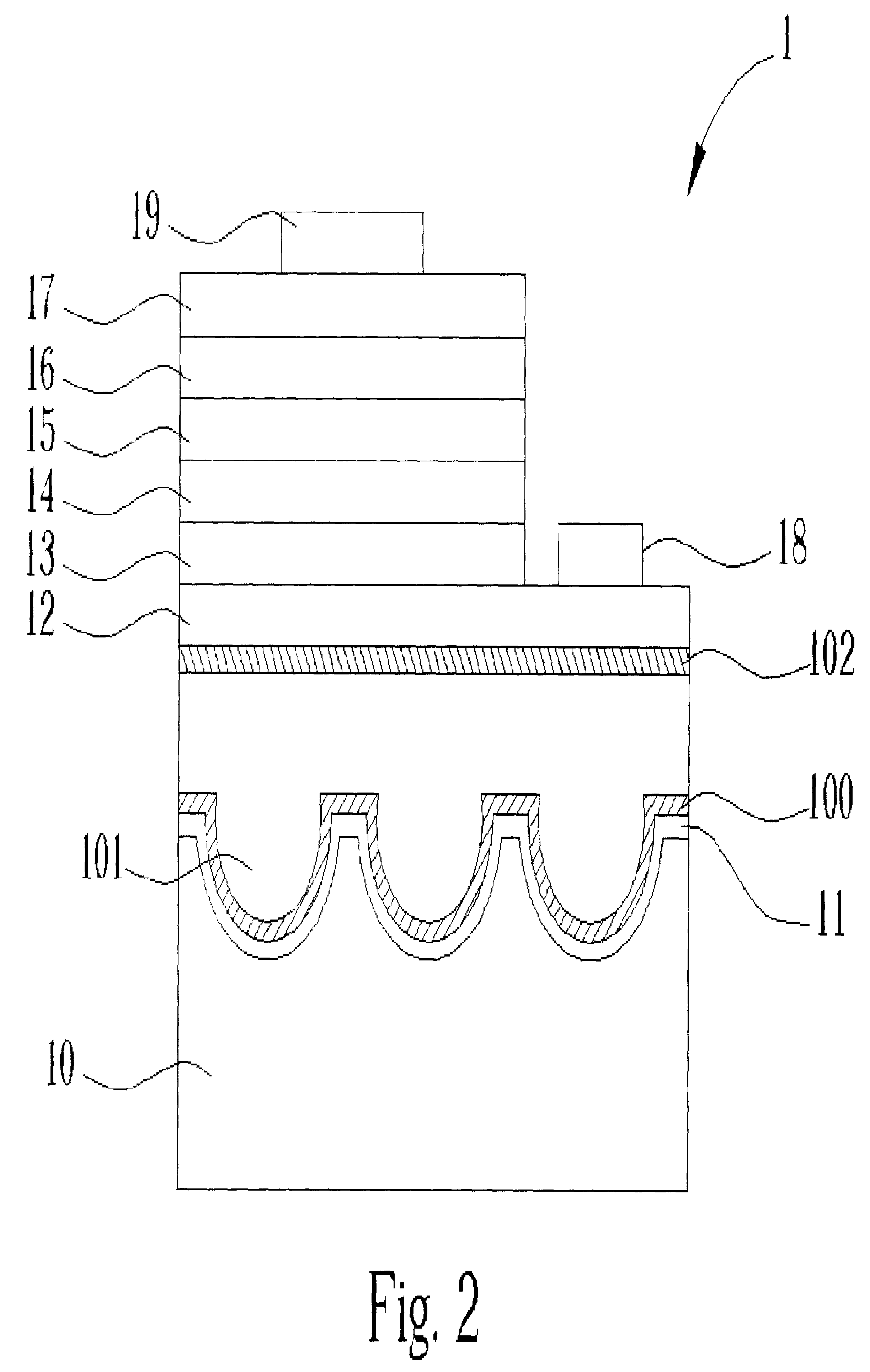
Figure 3
Abstract
Description
BACKGROUND OF INVENTION
[0001] 1. Field of the Invention
[0002] The present invention relates to a light emitting device, and more particularly, to a light emitting device with a micro-reflection structure carrier.
[0003] 2. Description of the Prior Art
[0004] Light emitting devices are extensively applied to many fields. For instance, light emitting devices are utilized in optical displays, laser diodes, traffic lights, data storages, communication devices, illumination devices, and medical instruments. For developing light emitting devices, one of the most important issues is to raise light emitting efficiency of light emitting devices.
[0005] In US publication No. US 2002 / 0017652 A1, an AlGaInP light emitting device of an embedded micro-reflection structure is disclosed. Please refer to FIG. 1. FIG. 1 is a prior art AlGaInP light emitting device of an embedded micro-reflection structure. LM is a metallic layer, CS is a conductive substrate, LE is an epitaxial layer with a micro-reflection ...
Examples
Embodiment Construction
[0015]Please refer to FIG. 2: FIG. 2 is a first embodiment of the present invention light emitting device with a micro-reflection structure carrier. 1 is a light emitting device with a micro-reflection structure carrier according to the present invention. 1 comprises a micro-reflection structure carrier 10, a reflection layer 11 formed over the micro-reflection structure carrier 10, a first reaction layer 100 formed over the reflection layer 11, a transparent adhesive layer 101 formed over the first reaction layer 100, a second reaction layer 102 formed over the transparent adhesive layer 101, a transparent conductive layer 12 formed over the second reaction layer 102, wherein a first surface area and a second surface are comprised on an upper surface of the transparent conductive layer 12, a first contact layer 13 formed over the first surface area, a first cladding layer 14 formed over the first contact layer 13, a light emitting layer 15 formed over the first cladding layer 14, a...