
Printed circuit board test access point structures and method for making the same
a technology of access point structure and printed circuit board, which is applied in the direction of printed circuit testing, inspection/indentification of circuits, instruments, etc., can solve the problems of increasing difficulty in hitting reliably and repeatably, increasing difficulty in matching length and symmetries, so as to reduce the width of the trace at the test access point
Patent Information
- Authority / Receiving Office
- US · United States
- Patent Type
- Patents(United States)
- Current Assignee / Owner
- Publication Date
- 2007-12-11
Smart Images
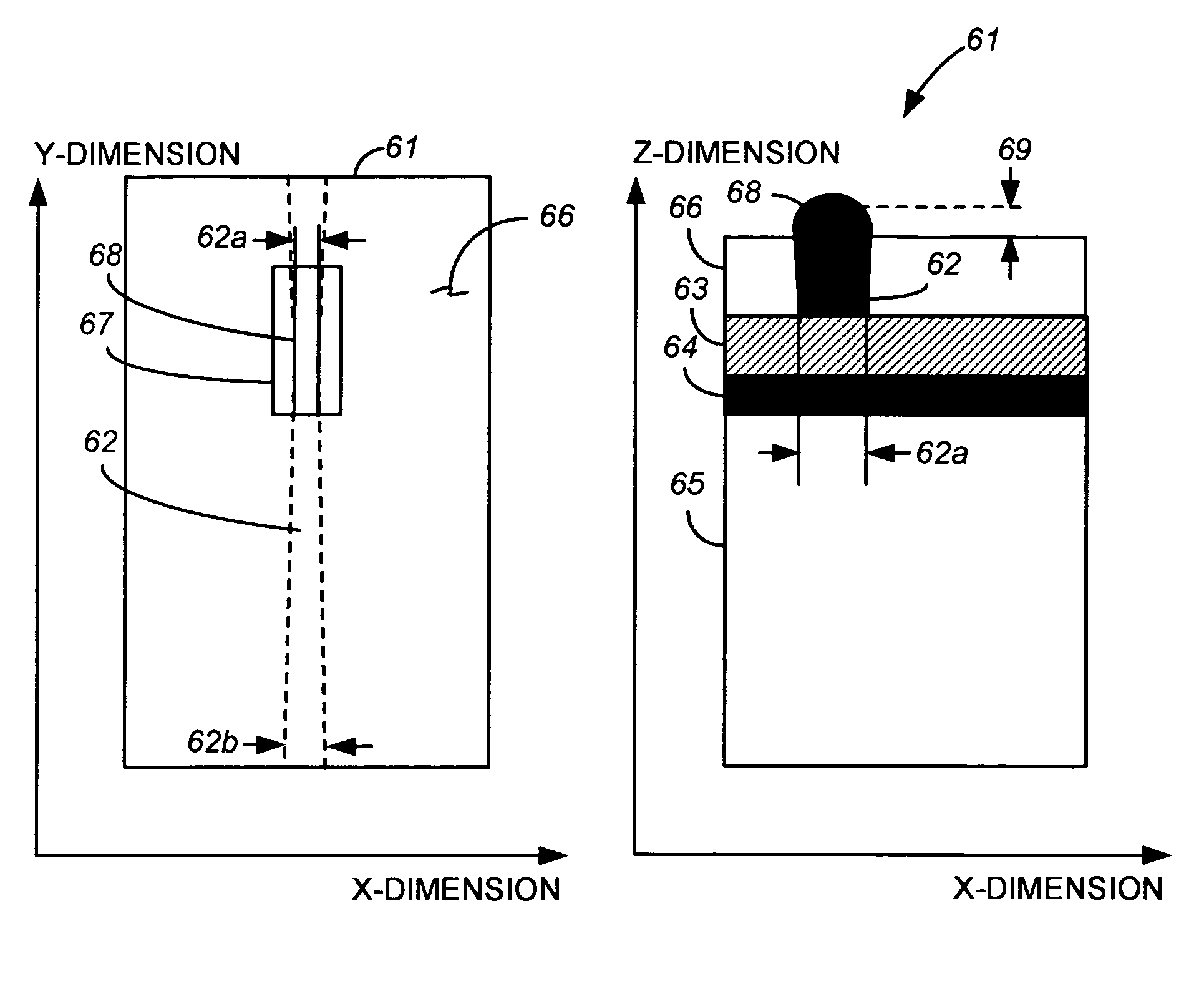
Figure 1 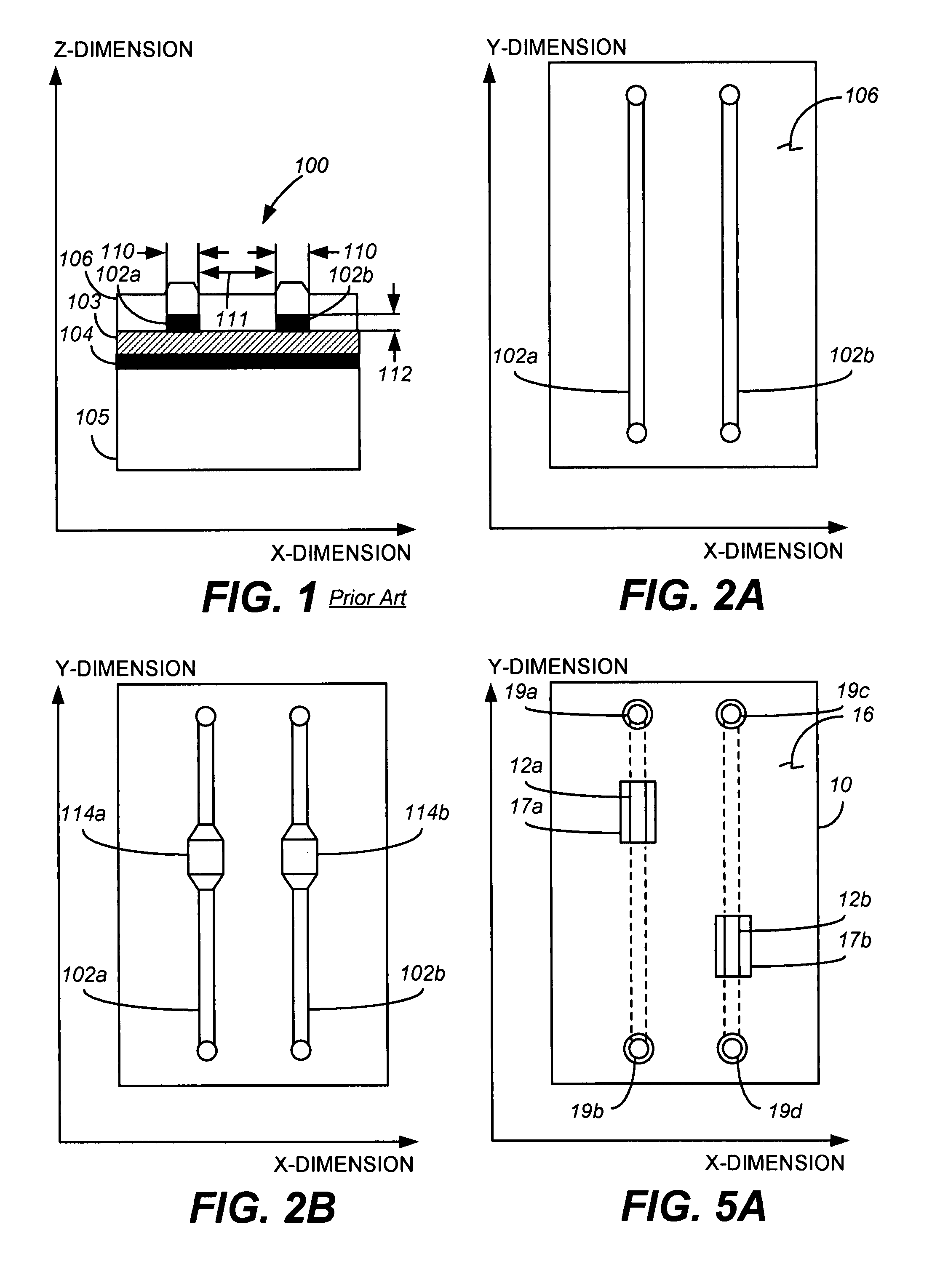
Figure 2 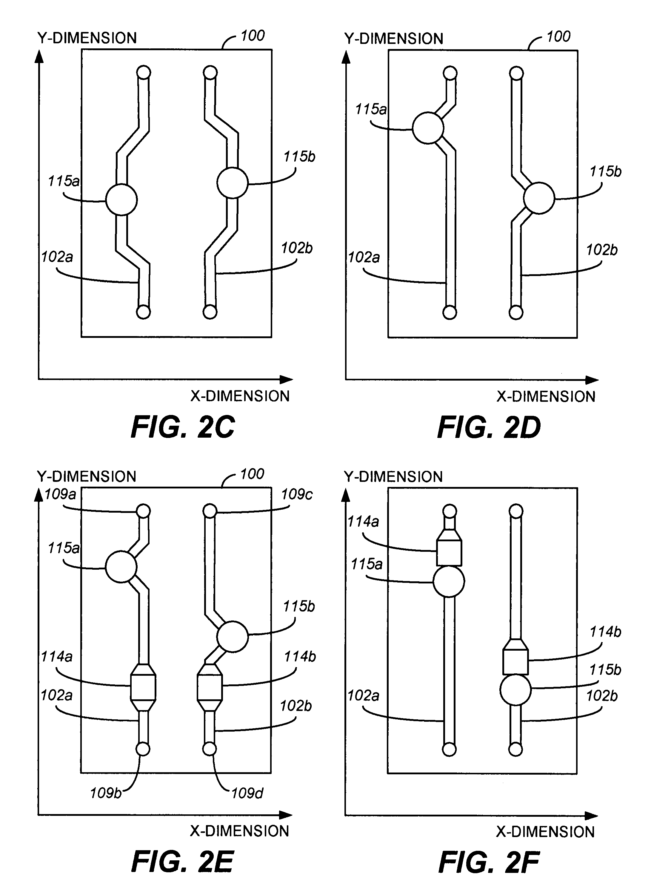
Figure 3
Abstract
Description
BACKGROUND OF THE INVENTION
[0001] In-circuit testers (ICT) have traditionally used “bed-of-nails” (BON) access to gain electrical connectivity to circuit wiring (traces, nets, pads) for control and observation capability needed for testing. This necessitates having access points within the layout of circuit nets that can be targets for ICT probes. Test access points are usually circular targets with 28 to 35 mil diameter that are connected to traces on the printed circuit board. In some cases these targets are deliberately added test pads, and in other cases the targets are “via” pads surrounding vias already provided in the printed circuit.
[0002] Lower diameter targets are increasingly difficult to hit reliably and repeatably, especially when a test fixture may contain several thousand such probes. It is always desirable to use larger diameter targets, but this is in fundamental conflict with the industry trend towards higher densities and smaller geometry devices.
[0003] Yet another i...
Examples
Embodiment Construction
[0043]Turning now in detail to the invention, on a trace defined in an x-, y-, z-coordinate system where the x-dimension represents the trace width, the y-dimension represents the trace length, and the z-dimension represents the trace thickness, it will be recognized by those skilled in the art that present techniques for test access point placement on a printed circuit board utilize only the x- and y-dimensions. The present invention takes a different approach by taking advantage of the z-dimension, that is, the trace thickness. In this regard, the test access point structure of the invention is a localized “high point” on a printed circuit board trace that does not significantly perturb the impedance of the trace and that can be targeted with a probe.
[0044]FIGS. 3A-3C illustrate an exemplary embodiment of a test access point structure implemented in accordance with the invention. As shown in FIGS. 3A-3C, a printed circuit board 1 includes a substrate 5, a ground plane 4, and at le...