
Method of manufacturing a metal substrate for an oxide superconducting wire
a metal substrate and superconducting wire technology, applied in the direction of superconducting magnets/coils, magnetic bodies, conductors, etc., can solve the problems of not taking into account the enhancement of orientation of oxide crystals, failing to obtain satisfactory critical current density, and slow forming rate, etc., to achieve excellent orientation, high critical current density, and excellent orientation
Patent Information
- Authority / Receiving Office
- US · United States
- Patent Type
- Patents(United States)
- Current Assignee / Owner
- Publication Date
- 2008-10-07
Smart Images
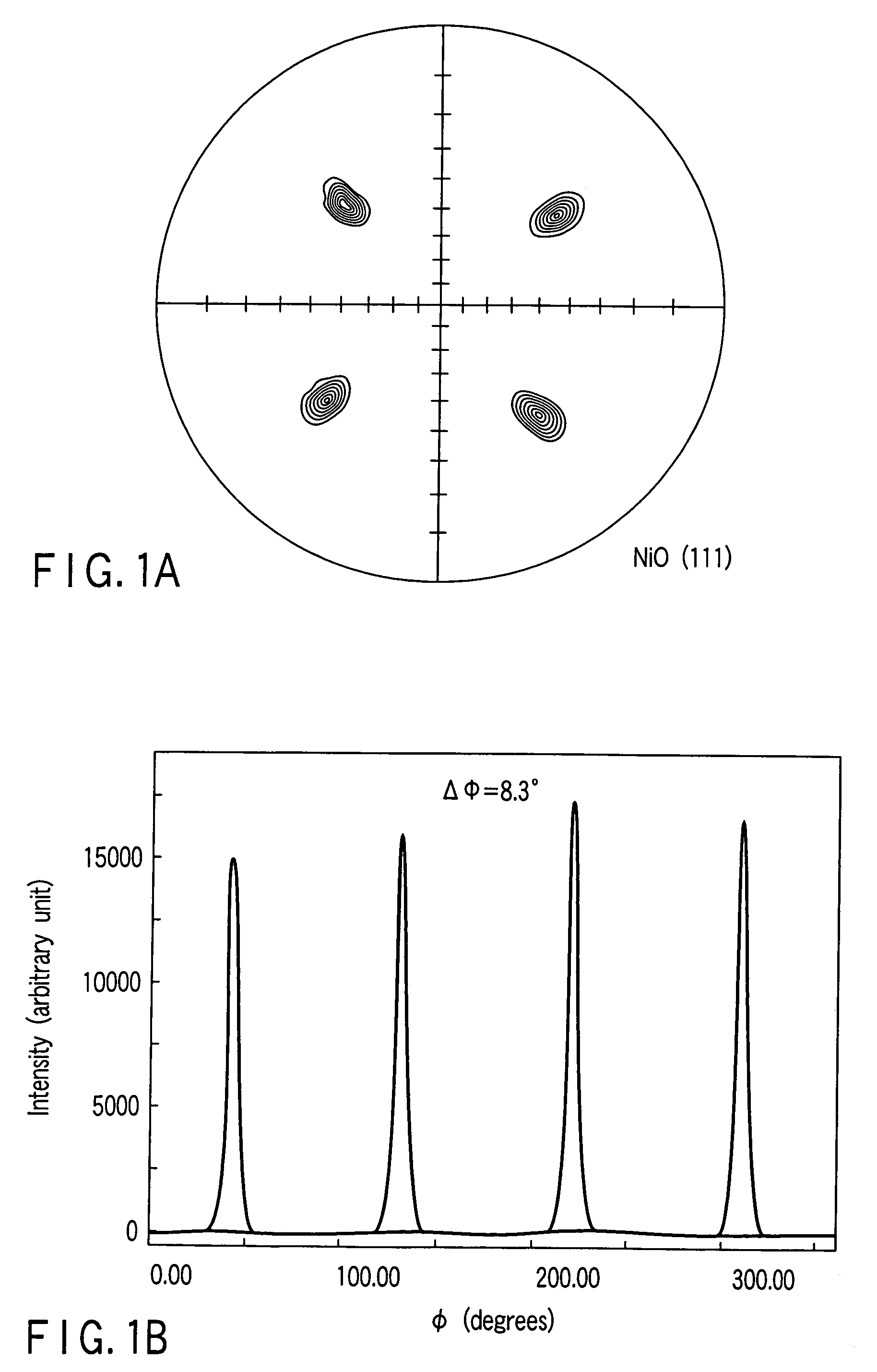
Figure 1 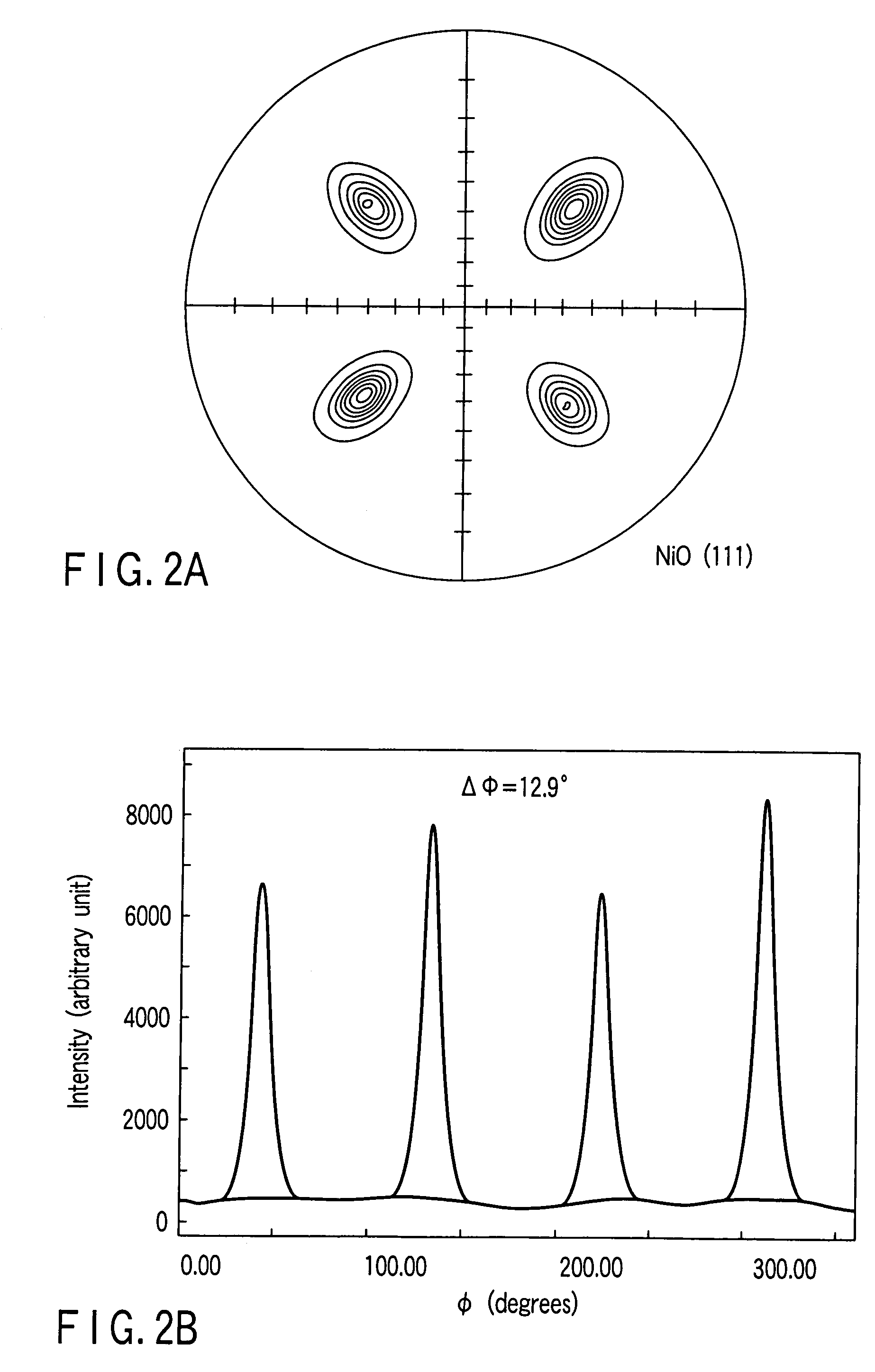
Figure 2 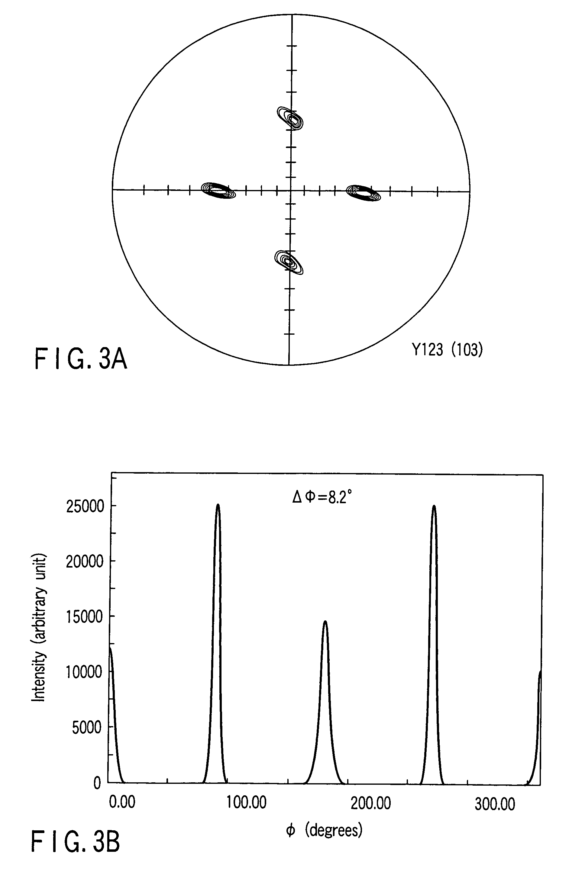
Figure 3
Abstract
Description
CROSS REFERENCE TO RELATED APPLICATIONS
[0001] This is a Continuation Application of PCT Application No. PCT / JP2004 / 004587, filed Mar. 31, 2004, which was published under PCT Article 21(2) in Japanese.
[0002] This application is based upon and claims the benefit of priority from prior Japanese Patent Application No. 2003-094792, filed Mar. 31, 2003, the entire contents of which are incorporated herein by reference.BACKGROUND OF THE INVENTION
[0003] 1. Field of the Invention
[0004] The present invention relates to a metal substrate for an oxide superconducting wire, an oxide superconducting wire, and a method of manufacturing the oxide superconducting wire.
[0005] 2. Description of the Related Art
[0006] As for the method of manufacturing a superconducting wire by making use of an oxide superconductor, there is known a method wherein an intermediate layer having a controlled crystal orientation is formed on an elongated metal tape, and an oxide superconducting layer is formed on the intermediate...
Examples
example 1
[0054]A polycrystalline nickel substrate having a rolled aggregate structure having a {100} plane which is parallel to the rolled surface and a axis which is parallel to the rolling direction was prepared. This substrate was placed in a heating furnace and subjected to a first heat treatment for 20 hours at a temperature of 750° C. and in an atmosphere containing a minute quantity of oxidizing gas created by continuously evacuating the heating furnace while introducing argon gas therein. Incidentally, when an average film-forming speed of this first heat treatment was measured, it was 0.15 μm / hr.
[0055]Although an NiO layer excellent in orientation was already formed at this stage, the thickness thereof was as thin as not more than 3 μm, so that it was most probable that the NiO layer would be vanished as the surface thereof was polished. Therefore, in order to secure the thickness of the NiO layer, a second stage heat treatment was performed as follows.
[0056]Namely, the polycrystal...
example 2
[0060]A polycrystalline nickel substrate having a rolled aggregate structure having a {100} plane which is parallel to the rolled surface and a axis which is parallel to the rolling direction was prepared. This substrate was placed in a heating furnace and subjected to a first heat treatment for one hour at a temperature of 1100° C. and in an atmosphere containing a minute quantity of oxidizing gas created by continuously evacuating the heating furnace while introducing argon gas therein.
[0061]Although an NiO layer excellent in orientation was already formed at this stage, the thickness thereof was as thin as not more than 1 μm, so that it was most probable that the NiO layer would be vanished as the surface thereof was polished. Therefore, in order to secure the thickness of the NiO layer, a second stage heat treatment was performed as follows.
[0062]Namely, the polycrystalline nickel substrate having a thin NiO film formed thereon by the first heat treatment was further subjected ...
example 3
[0068]The surface of the substrate obtained in Example 1 was buffed to obtain a polished surface on which a BaZrO3 film was formed as a diffusion barrier layer by means of laser abrasion using KrF excimer laser. The deposition of the BaZrO3 film was performed in an Ar gas atmosphere of 20 mm Torr in pressure with the repeating frequency of laser being set to the range of 10-20 Hz and the temperature of the substrate being controlled to 600-700° C.
[0069]On this diffusion barrier layer formed in this manner, a Y123 oxide superconductor layer was formed by means of laser abrasion. The deposition of the Y123 oxide superconductor layer was performed in an O2 gas atmosphere of 100-200 mm Torr in pressure with the repeating frequency of laser being set to the range of 10-20 Hz and the temperature of the substrate being controlled to 700-800° C.
[0070]On this Y123 oxide superconductor layer was further deposited a Y—Yb123 oxide superconductor layer by means of liquid phase epitaxy. More spec...