
Manufacturing method for a semiconductor device
a manufacturing method and semiconductor technology, applied in the direction of semiconductor/solid-state device details, digital storage, instruments, etc., can solve the problems of excessive stress on the portions, damage to cracks formed by minute fissures on the rear surface of the semiconductor wafer, so as to improve the strength and thinning effect and improve reliability
Patent Information
- Authority / Receiving Office
- US · United States
- Patent Type
- Patents(United States)
- Current Assignee / Owner
- Publication Date
- 2008-11-25
Smart Images
Figure 1 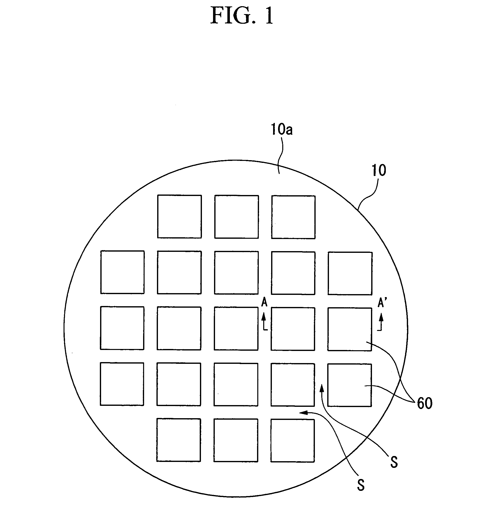
Figure 2 
Figure 3
Abstract
Description
CROSS-REFERENCE TO RELATED APPLICATION
[0001] This application claims priority to Japanese Patent application No. 2005-177495, filed Jun. 17, 2005, and Japanese Patent application No. 2005-335459, filed Nov. 21, 2005, the contents of which are incorporated herein by reference.BACKGROUND
[0002] 1. Technical Field
[0003] The present invention relates to the manufacturing method for a semiconductor device, a semiconductor device, a circuit substrate and an electronic device.
[0004] 2. Related Art
[0005] In recent years, there has been a demand to miniaturize and reduce the weight of portable telephone devices, notebook portable computers and portable electronic devices such as a PDA (personal digital assistant) and the similar.
[0006] Accompanying the demand for miniaturization and weight reduction, there has also been demand to limit the packaging space for each type of electronic product, such as semiconductor devices and the similar, provided within the electronic devices, as well as to miniatu...
Examples
first embodiment
[0107]Semiconductor Wafer
[0108]First of all, an explanation is provided concerning the semiconductor wafer before the individualizing of the semiconductor devices.
[0109]FIG. 1 is a plan view that schematically shows the semiconductor wafer 10 on which a plurality of semiconductor regions 60 is formed.
[0110]Semiconductor wafer 10 is formed from silicon material on which is formed semiconductor regions 60.
[0111]On the active surface 110a of the semiconductor wafer 1 is formed an accumulation circuit (integrated circuit) including a transistor, memory element and other semiconductor elements for each of the semiconductor regions 60.
[0112]In the first embodiment, the semiconductor region 60 is a region which becomes a semiconductor device by below described manufacturing method, and means a region formed on a semiconductor wafer before the individualizing of the semiconductor devices.
[0113]The semiconductor element is not formed on the rear surface 10b of the opposite side of the active...
second embodiment
[0225]An explanation of the second embodiment is provided hereafter, with reference to the drawings.
[0226]In the second embodiment, the first groove 20 is filled with resin, and a resin layer is formed into the first groove 20.
[0227]Therefore, the manufacturing process of the semiconductor device 61 of the second embodiment differs from the manufacturing process of the semiconductor device 61 of the first embodiment.
[0228]In the second embodiment, a detailed explanation is provided concerning the forming process of a resin layer into the first groove 20, and a process after the forming process of a resin layer within the first groove 20.
[0229]The same reference numerals are applied to construction components which are common to those of the semiconductor device 61 of the first embodiment, simplifying the explanation of other processes.
[0230]Electrode and First Groove Forming Processes
[0231]First of all, as shown in FIG. 5A, electrode pad 14 is formed on the semiconductor wafer 10 on...
third embodiment
[0278]An explanation of this embodiment is provided next, with reference to the drawings.
[0279]In the manufacturing method for the semiconductor device 61 of the third embodiment, there is a difference in comparison with the manufacturing method for the semiconductor device 61 of the first embodiment, in the point that TEG is not formed in the respective cutting regions S of semiconductor regions 60 in the semiconductor wafer.
[0280]In the third embodiment, the same reference numerals are applied to and explanations omitted from processes and compositions which are the same as those of the first embodiment, and explanations are only provided for parts which differ from those of the first embodiment.
[0281]FIGS. 8A to 9C are cross-sectional views that show the forming of semiconductor devices 61 in which the semiconductor wafer 10 has been individualized for each semiconductor region 60.
[0282]Semiconductor Wafer
[0283]First of all, an explanation is provided concerning semiconductor waf...