
Mirror device
a mirror device and light modulator technology, applied in the field of mirror devices, can solve the problems of adverse effects on image quality, limited image display quality, and limited image quality, so as to prevent adverse effects and improve device configurations.
Patent Information
- Authority / Receiving Office
- US · United States
- Patent Type
- Patents(United States)
- Current Assignee / Owner
- Publication Date
- 2010-01-26
Smart Images
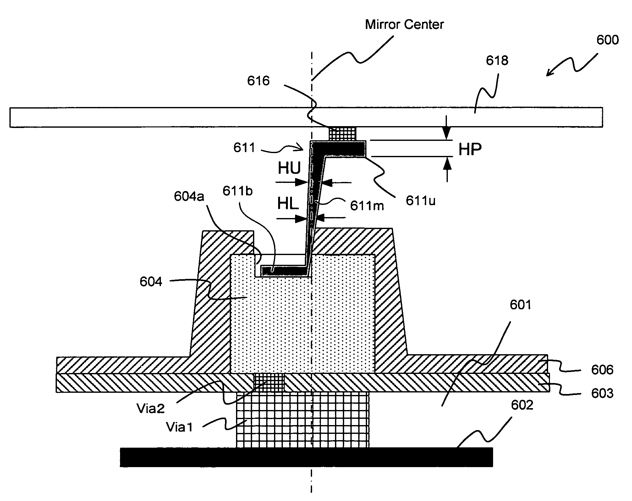
Figure 1 
Figure 2 
Figure 3
Abstract
Description
CROSS REFERENCE TO RELATED APPLICATIONS
[0001] This application is Continuation in Part (CIP) Application of a Co-Pending patent application Ser. No. 11 / 894,248 filed on Aug. 18, 2007 by one of the common Inventors of this patent application. Application Ser. No. 11 / 894,248 is a Non-provisional application of a Provisional application 60 / 841,173 filed on Aug. 30, 2006. The Provisional Application 60 / 839,637 is a Continuation in Part (CIP) Application of a pending U.S. patent application Ser. Nos. 11 / 121,543 filed on May 4, 2005. The application Ser. No. 11 / 121,543 is a Continuation in part (CIP) Application of three previously filed Applications. These three Applications are U.S. application Ser. Nos. 10 / 698,620 filed on Nov. 1, 2003, 10 / 699,140 filed on Nov. 1, 2003, and 10 / 699,143 filed on Nov. 1, 2003 by one of the Applicants of this patent application. The disclosures made in these patent applications are hereby incorporated by reference in this patent application.BACKGROUND OF TH...
Examples
Embodiment Construction
[0077]A mirror device implemented in a projection apparatus according to a preferred embodiment of the present invention is described below by referring to the accompanying drawings.
[0078]FIGS. 5A through 5F are cross-sectional diagrams for describing the processing steps for producing a mirror device according to a preferred embodiment of the present invention.
[0079]FIG. 5A shows the step 1 to form a wiring 502 of a drive circuit for driving and controlling a mirror (which is described later) in a semiconductor wafer substrate (simply noted as “substrate” hereinafter) 501. A cavity as an opening part (i.e., a cavity or concave part) 501a is opened from a top surface of the substrate 501 and extends to the upper surface of the wiring 502 preferably composed of aluminum. A first protective layer, i.e., a protective film, 503 is deposited on the parts of the substrate 501 except for the opening part 501a. The first protective layer 503 is deposited before the opening part 501a of the ...