
Shielded gate mosfet-schottky rectifier-diode integrated circuits with trenched contact structures
a technology of integrated circuits and contact structures, which is applied in the direction of diodes, semiconductor devices, electrical apparatus, etc., can solve the problems of poor performance and high manufacturing cost, and achieve the effects of improving the configuration of semiconductor power devices, reducing die size and cos
Patent Information
- Authority / Receiving Office
- US · United States
- Patent Type
- Applications(United States)
- Current Assignee / Owner
- Publication Date
- 2013-01-24
Smart Images
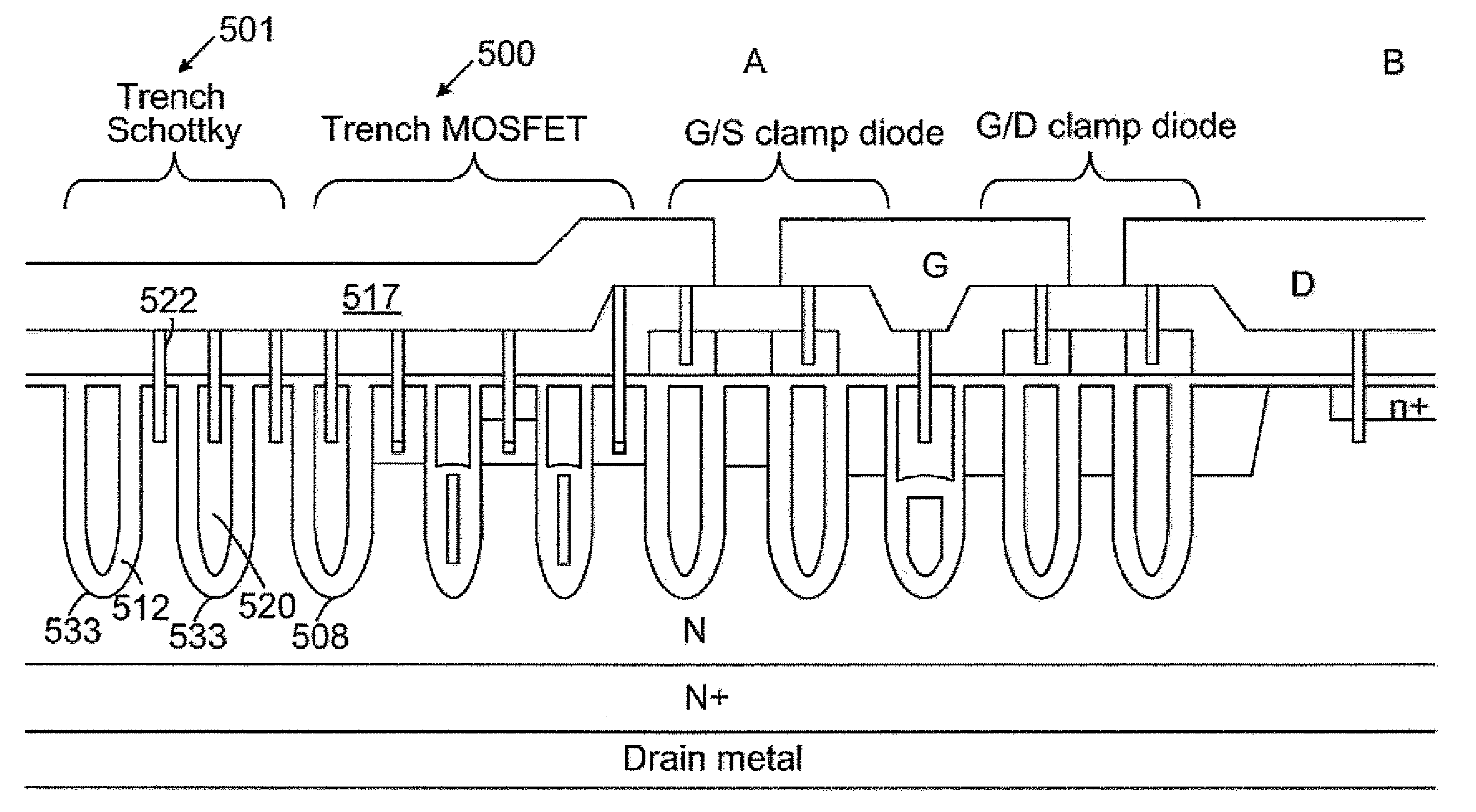
Figure 1 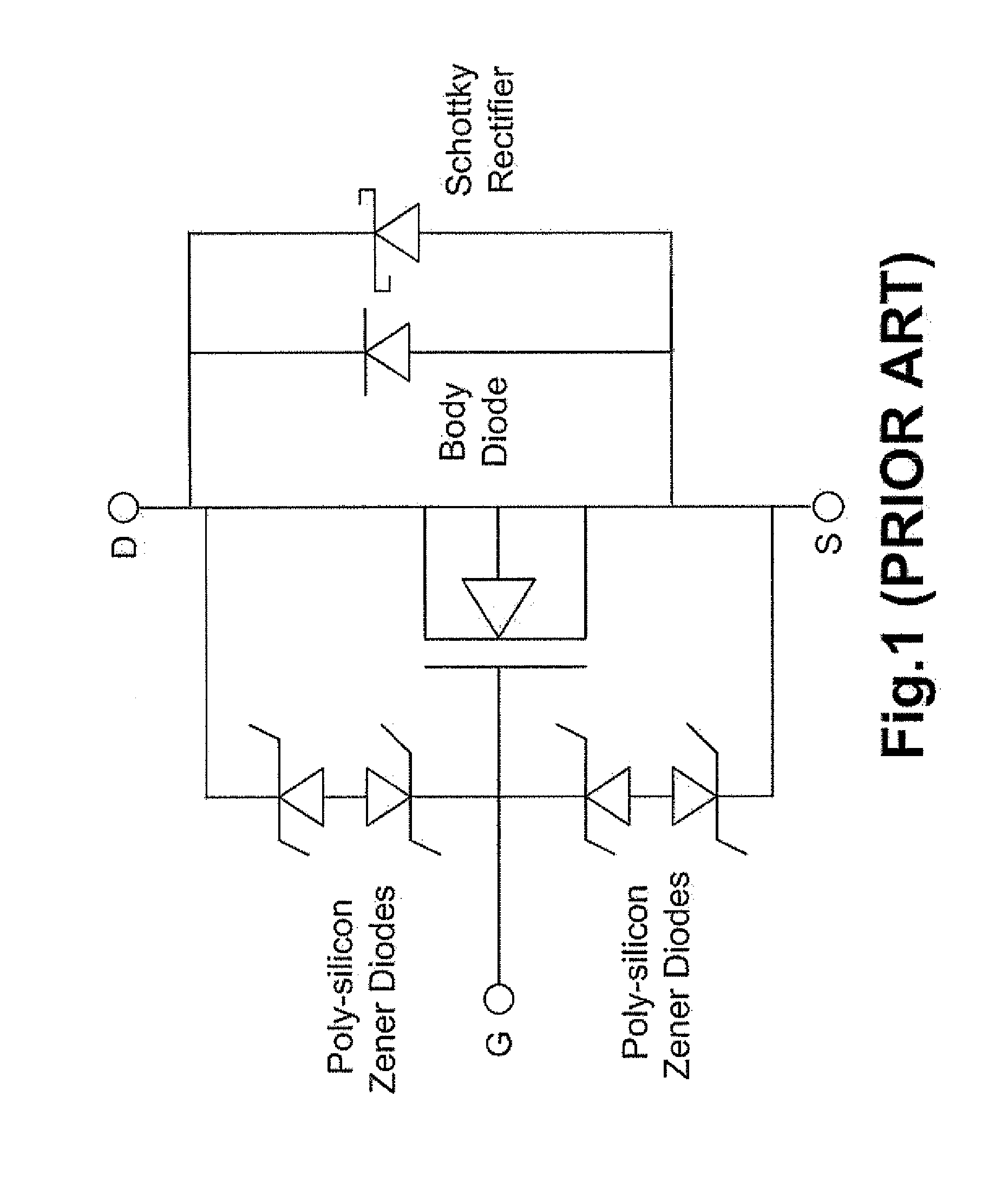
Figure 2 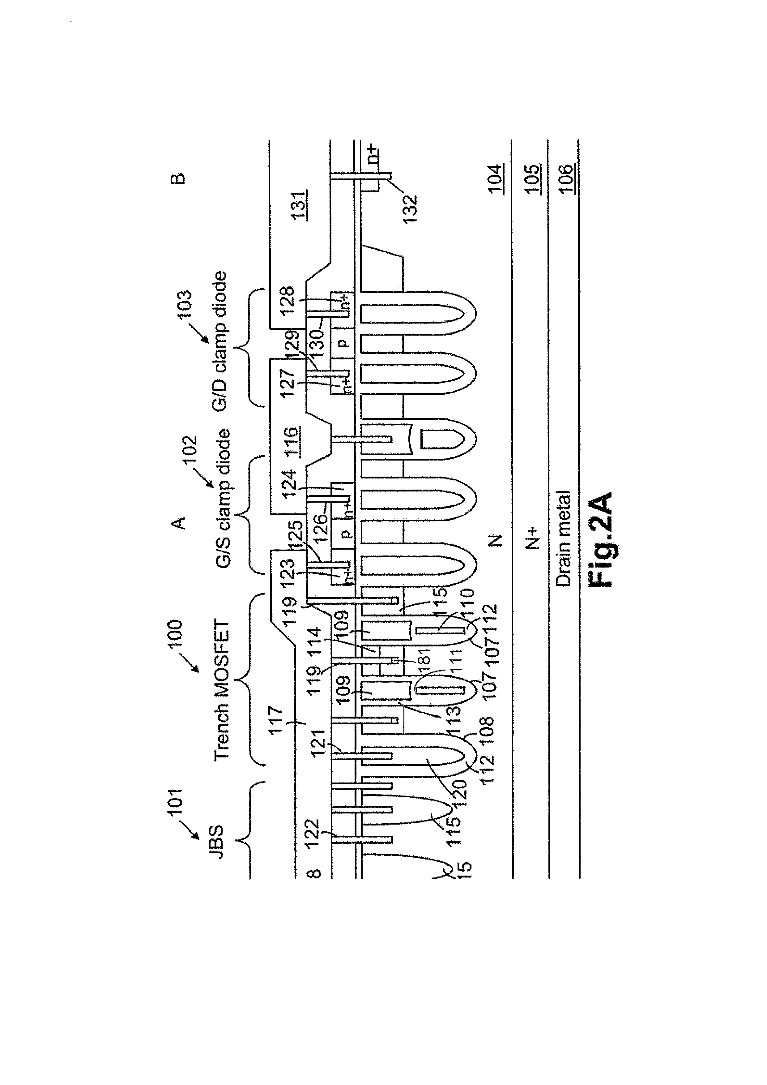
Figure 3
Abstract
Description
FIELD OF THE INVENTION
[0001] This invention relates generally to the cell structure, device configuration and fabricating method of power semiconductor devices. More particularly, this invention relates to an improved cell configuration to manufacture trench shielded gate MOSFET (Metal Oxide Semiconductor Field Effect Transistor) with Schottky rectifier diode, Gate-Drain (GD) and Gate-Source (GS) clamp diode on single chip for device shrinkage and performance improvement.BACKGROUND OF THE INVENTION
[0002] Please refer to FIG. 1, normally for high efficiency DC / DC application, a Schottky rectifier is externally added in parallel with a MOSFET device to prevent a parasitic P / N body diode in the MOSFET from turning on in order to achieve higher speed and efficiency. The requirement for clamping effect is that the forward voltage of the Schottky rectifier Vf is less than the parasitic P / N body diode (˜0.7V). Besides, for providing effective ESD (electrostatic discharge) protection between ...
Examples
Embodiment Construction
[0021]Please refer to FIG. 2A and FIG. 2B for a preferred embodiment of this invention which is respective A-B and C-D cross-sectional view of FIG. 2C. In FIG. 2A, an N-channel trench MOSFET 100 is implemented with Junction Barrier Schottky rectifier 101 (JBS, as illustrated), a Gate-Source clamp diode 102 (GIS clamp diode, as illustrated) and a Gate-Drain clamp diode 103 (G / D clamp diode, as illustrated) in an N epitaxial layer 104 above an N+ substrate 105 which is coated with back metal of Ti / Ni / Ag on rear side as drain metal 106. The trench MOSFET 100 further comprises a plurality of first type gate trenches 107 for shielded trenched gates and a second type gate trench 108 for shielded electrode contact, wherein each the first type gate trench 107 is filled with a gate electrode 109 in the upper portion and a shielded electrode 110 in the lower portion, wherein the gate electrode 109 is insulated from the shielded electrode 110 by an inter-electrode insulation layer 111. Besides...