
Super-junction trench mosfet integrated with embedded trench schottky rectifier
a super-junction trench and rectifier technology, applied in semiconductor devices, diodes, electrical apparatuses, etc., can solve the problems of high power dissipation, large electro-magnetic interference (emi) noise, and hard body diode reverse recovery operation, so as to improve device performance, improve device configuration, and improve device performance
Patent Information
- Authority / Receiving Office
- US · United States
- Patent Type
- Applications(United States)
- Current Assignee / Owner
- Publication Date
- 2016-04-14
- Estimated Expiration
- Not applicable · inactive patent
Smart Images
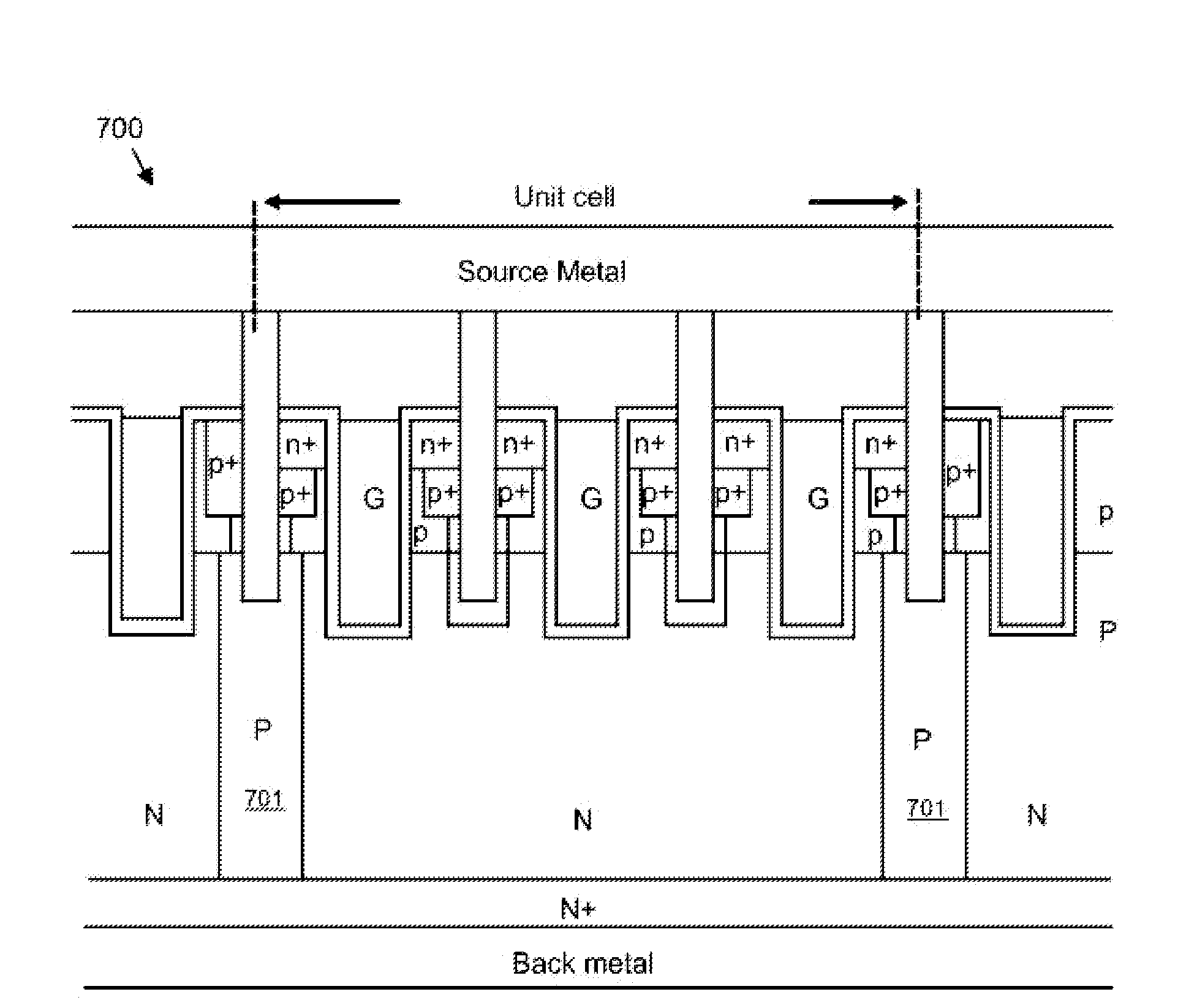
Figure 1 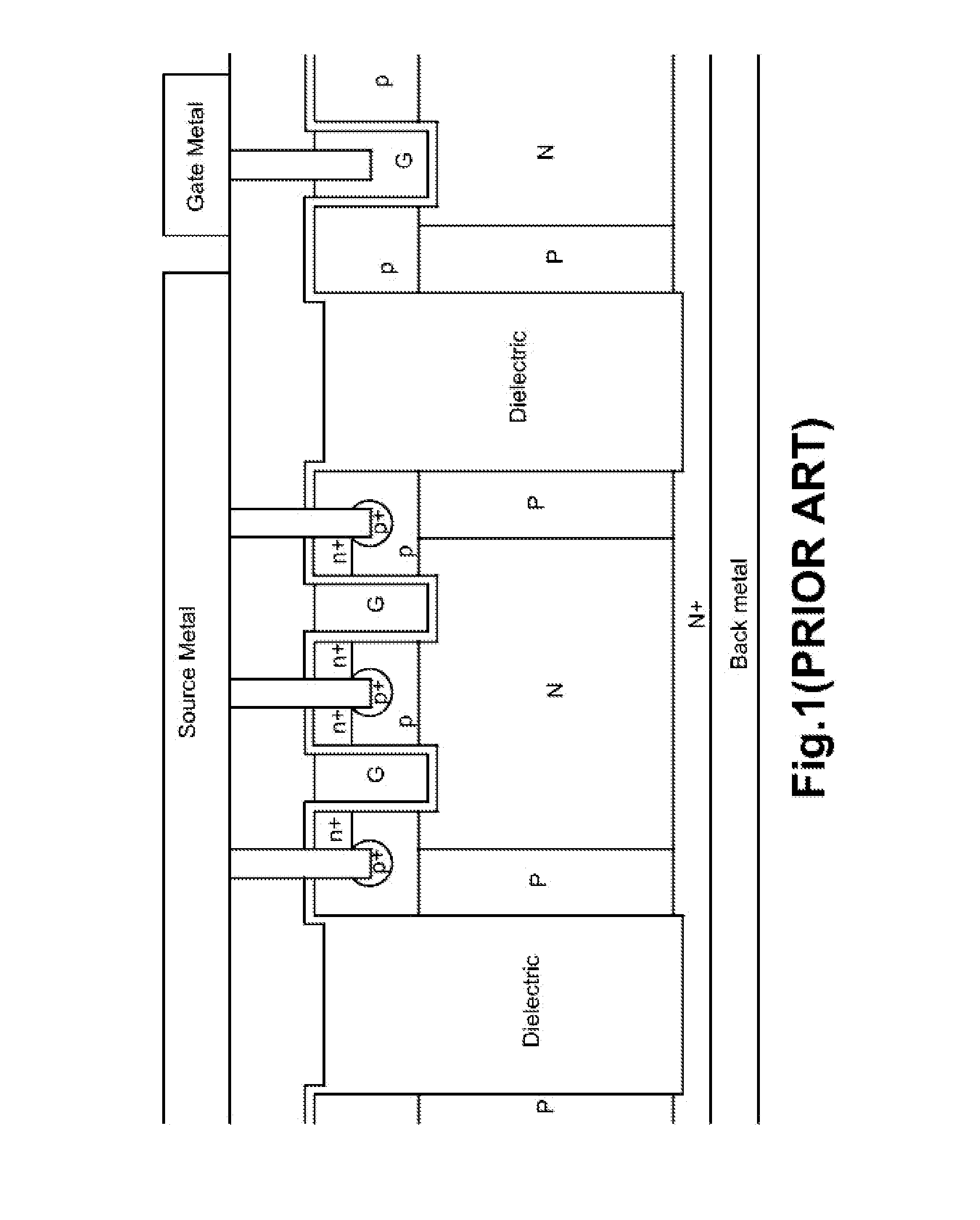
Figure 2 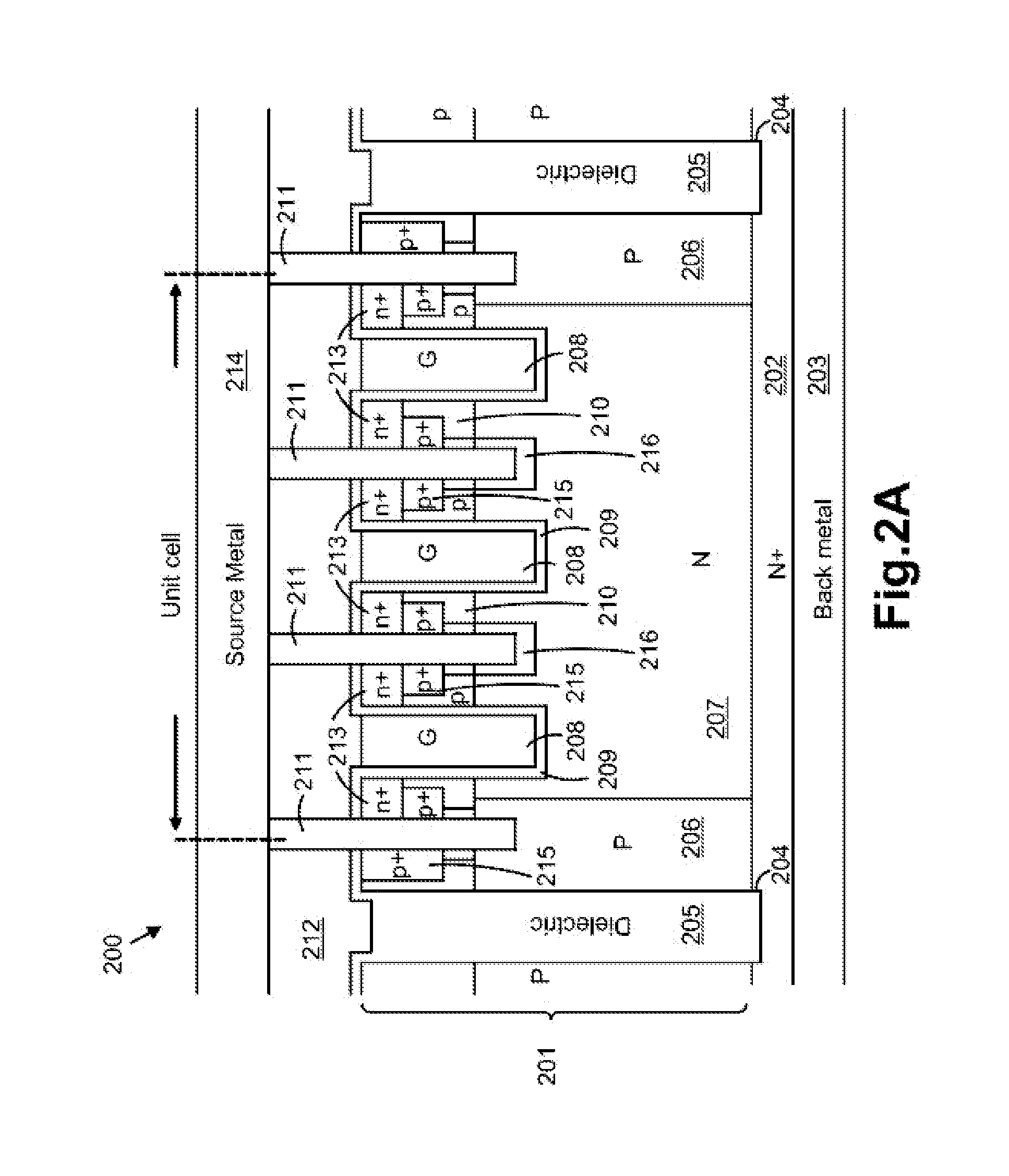
Figure 3
Abstract
Description
FIELD OF THE INVENTION
[0001] This invention relates generally to the cell structure, device configuration of power semiconductor devices. More particularly, this invention relates to a novel and improved cell structure, device configuration of a super-junction trench MOSFET (Metal Oxide Semiconductor Field Effect Transistor, the same hereinafter) integrated with embedded trench Schottky rectifierBACKGROUND OF THE INVENTION
[0002] Compared to the conventional trench MOSFETs, super-junction trench MOSFETs are more attractive due to its better performance. For example, FIG. 1 shows a super-junction trench MOSFET disclosed in U.S. application Ser. No. 13 / 568,297 (having the same inventor as the present invention), which also contains multiple trenched gates in unit cell and has advantages such as: higher breakdown voltage, lower specific Rds (drain-source resistance), minimized influence of charge imbalance, better UIS (unclamped inductive switching) capability . . . etc., especially for s...
Examples
Embodiment Construction
[0020]In the following Detailed Description, reference is made to the accompanying drawings, .which forms a part thereof, and in which is shown by way of illustration specific embodiments in which the invention may be practiced. In this regard, directional terminology, such as “top”, “bottom”, “front”, “back”, etc., is used with reference to the orientation of the Figure(s) being described. Because components of embodiments can be positioned in a number of different orientations, the directional terminology is used for purpose of illustration and is in no way limiting. It is to be understood that other embodiments may be utilized and structural or logical changes may be make without departing from the scope of the present invention. The following detailed description, therefore, is not to be taken in a limiting sense, and the scope of the present invention is defined by the appended claims. It is to be understood that the features of the various exemplary embodiments described herei...