
Etching method and etching equipment
a technology of etching equipment and etching method, which is applied in the direction of electrical equipment, decorative surface effects, decorative arts, etc., can solve the problems of ion bombardment damage to the tapered portion of the trench, damage to the surface protection of the upper portion of the side walls, so as to achieve rapid increase of reaction rate, high etching rate, and maintain throughput
Patent Information
- Authority / Receiving Office
- US · United States
- Patent Type
- Patents(United States)
- Current Assignee / Owner
- Publication Date
- 2012-10-16
Smart Images
Figure 1 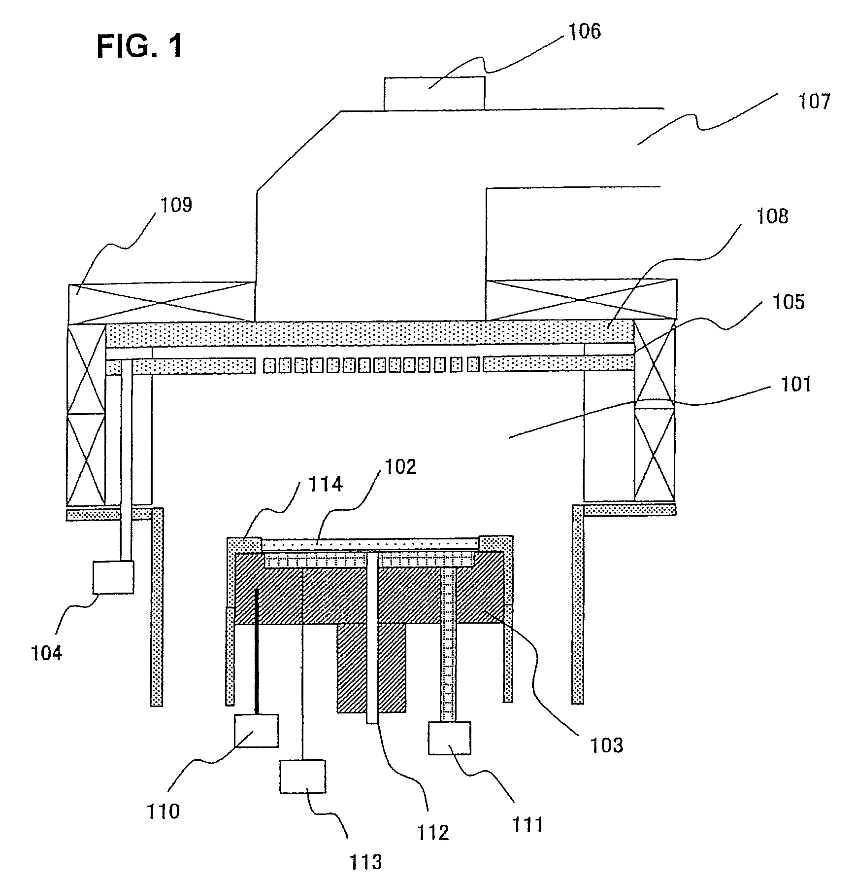
Figure 2 
Figure 3
Abstract
Description
[0001] The present application is based on and claims priority of Japanese patent application No. 2005-295462 filed on Oct. 7, 2005, the entire contents of which are hereby incorporated by reference. This application is a Divisional application of prior application Ser. No. 11 / 288,105, filed Nov. 29, 2005 now abandoned, the contents of which are incorporated herein by reference in their entirety.BACKGROUND OF THE INVENTION
[0002] 1. Field of the Invention
[0003] The present invention relates to a method and equipment for etching a semiconductor device. More specifically, the present invention relates to a method and equipment capable of preventing the side walls of a trench (groove or hole) from being damaged.
[0004] 2. Description of the Related Art
[0005] Recently, silicon (Si) trench etching is applied as a device isolation technique to devices such as in-vehicle pressure-resistant IGBT (insulated gate bipolar transistor) devices corresponding to hybrid vehicles, which is drawing keen att...
Examples
embodiment 1
[0021]FIG. 1 shows a microwave plasma etching equipment according to embodiment 1 of the present invention utilizing microwaves and magnetic fields as means for generating plasma.
[0022]In the present equipment, etching gas is supplied to an etching processing chamber 101 from a gas supply means 104 via a permeation window 105 having a porous structure made of quartz, for example.
[0023]Further, microwaves generated from a microwave generator (not shown) are transmitted via a matching box 106 and a waveguide 107 and through a microwave introduction window 108 into the etching processing chamber 101 to turn the above-mentioned etching gas into plasma.
[0024]In order to enhance the radiation efficiency, a solenoid coil 109 for generating magnetic fields is disposed around the etching chamber, a magnetic field of 0.0875 T is generated, and high-density plasma is generated by the magnetic field utilizing electron cyclotron resonance. A sample stage 103 is disposed in the etching chamber 10...