
Crack-stopping structure and method for forming the same
a crackstopping structure and hollow structure technology, applied in semiconductor/solid-state device testing/measurement, semiconductor device details, semiconductor/solid-state device testing/measurement, etc., can solve the problem of serious peeling at the place the metal pattern occupies, and achieve the effect of preventing delamination and/or cracking, adversely affecting reliability and yield
Patent Information
- Authority / Receiving Office
- US · United States
- Patent Type
- Patents(United States)
- Current Assignee / Owner
- Publication Date
- 2016-08-30
Smart Images
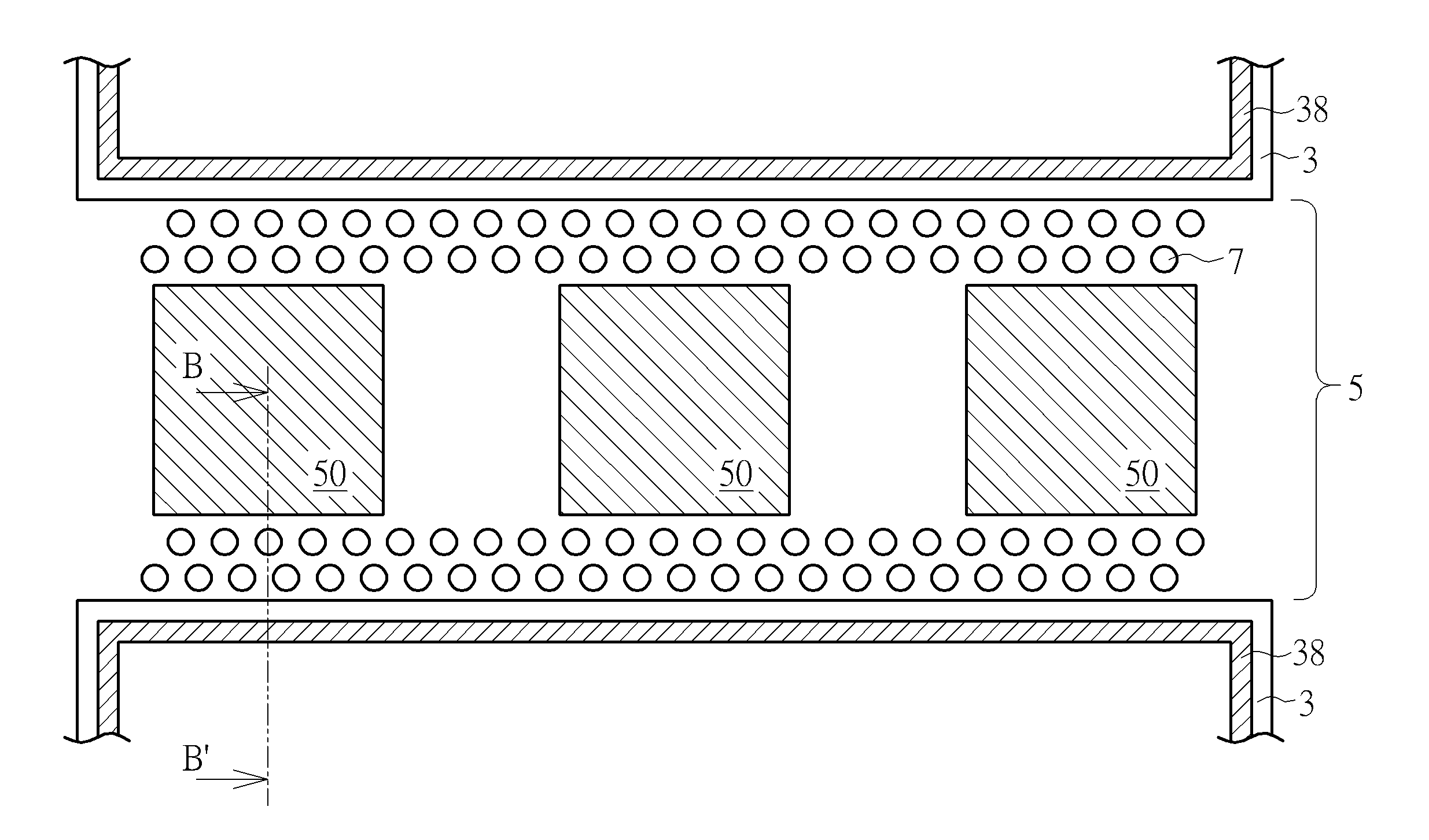
Figure 1 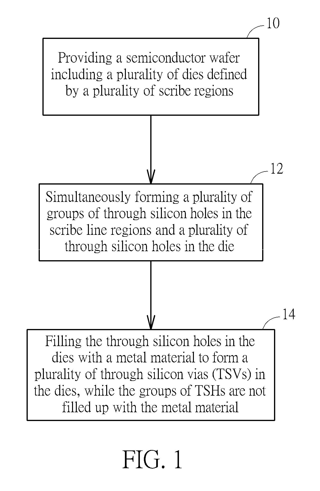
Figure 2 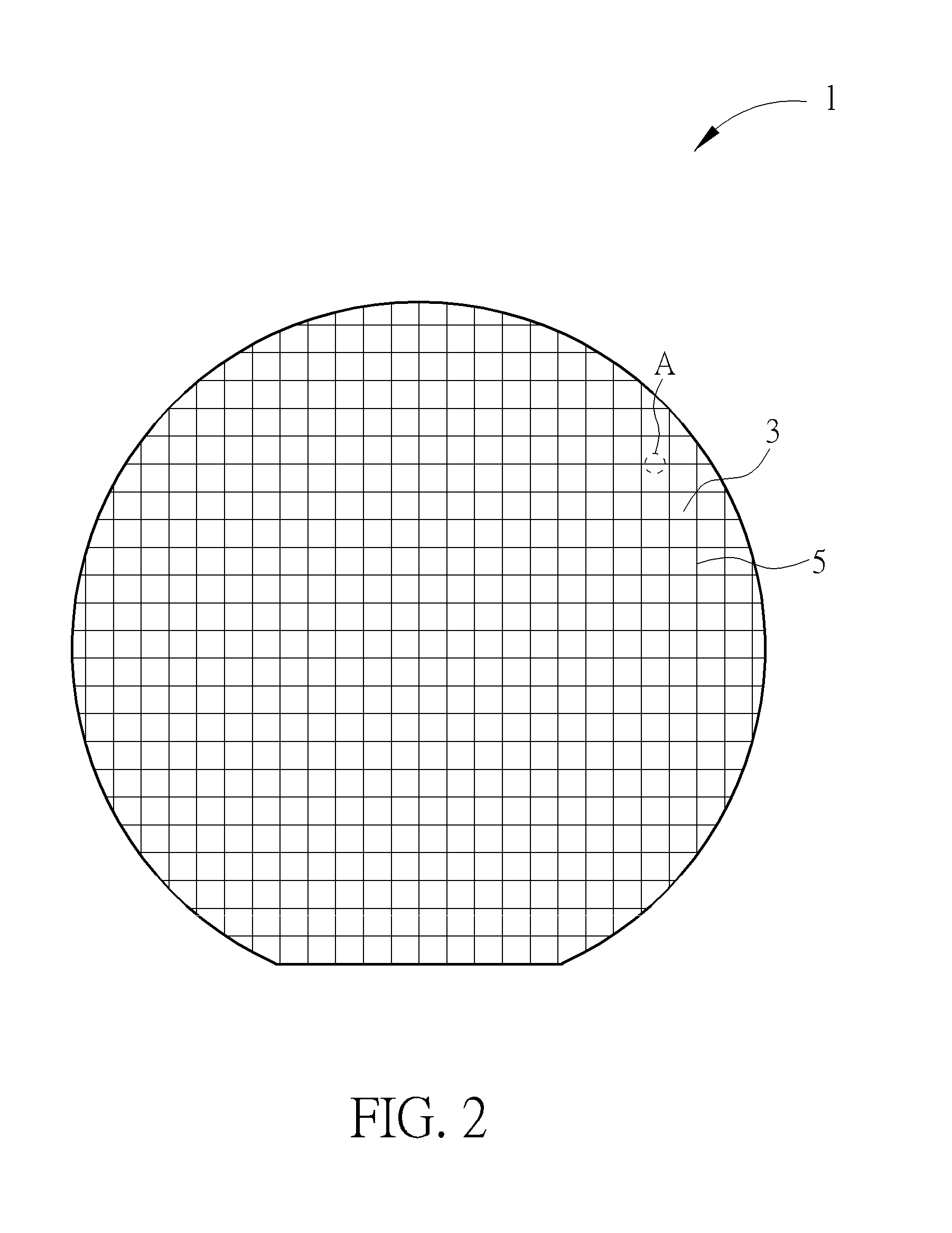
Figure 3
Abstract
Description
BACKGROUND OF THE INVENTION
[0001] 1. Field of the Invention
[0002] The invention relates to a crack-stopping structure and method for forming the same, and more particularly, to a wafer crack-stopping hollow structure and method for forming the same.
[0003] 2. Description of the Prior Art
[0004] In the field of semiconductor device fabrication, semiconductor devices and interconnections are formed to construct integrated circuits (ICs) on a semiconductor wafer. The fabrication of ICs may be completed through different methods and steps, but generally involves depositing layers of conductive, semiconductor, and insulating materials in precise patterns on a substrate or wafer to form the desired circuit or array patterns. Once formed, the ICs then need to be separated into individual piece-parts, so called dies or chips. The dies, which are isolated or separated from each other by scribe lines, are then separated by sawing along the scribe lines and are individually packaged.
[0005] When proce...
Examples
Embodiment Construction
[0022]Please refer to FIGS. 1-7. FIG. 1 is a flowchart illustrating a method for forming a crack-stopping structure provided by a first preferred embodiment of the present invention. FIGS. 2-7 are schematic drawings illustrating a method for forming a crack-stopping structure provided by the first preferred embodiment, wherein FIG. 2 is a plan view showing an overall configuration of a semiconductor wafer, FIG. 3 is a partially enlarged view of Circle A of FIG. 2, FIG. 4 is a cross-sectional view taken along a Line B-B′ of FIG. 3, FIG. 5 is a partially enlarged view of Circle A of FIG. 2 and in a step subsequent to FIG. 3, and FIGS. 6-7 are cross-sectional views taken along a Line B-B′ of FIG. 5. As shown in FIG. 1, the method for forming a crack-stopping structure first provides a Step 10:
STEP 10: Providing a semiconductor wafer comprising a plurality of dies defined by a plurality of scribe line regions.
[0023]In order to clearly describe the structure of the present invention, FIG...