Advancements in Silver Nanowire Conductive Inks for Printing
SEP 25, 202510 MIN READ
Generate Your Research Report Instantly with AI Agent
Patsnap Eureka helps you evaluate technical feasibility & market potential.
Silver Nanowire Conductive Inks Background and Objectives
Silver nanowire (AgNW) conductive inks represent a significant advancement in the field of printed electronics, emerging as a promising alternative to traditional indium tin oxide (ITO) and other conductive materials. The development of these inks can be traced back to the early 2000s, when researchers began exploring nanomaterials for flexible electronics applications. The evolution of AgNW technology has been driven by increasing demands for transparent conductive films in touch screens, displays, photovoltaics, and wearable electronics.
The fundamental appeal of silver nanowires lies in their unique combination of electrical conductivity and optical transparency. Silver, as a noble metal, offers the highest electrical conductivity among all elements, while the nanowire morphology enables the formation of percolating networks that maintain conductivity even at low material loadings. This characteristic has positioned AgNW inks as a key enabling technology for next-generation flexible, stretchable, and transparent electronic devices.
Technical evolution in this field has progressed through several distinct phases. Initial research focused on synthesis methods to control nanowire dimensions and aspect ratios, primarily using polyol processes. Subsequent developments addressed ink formulation challenges, including dispersion stability, rheological properties, and compatibility with various printing techniques. Recent advancements have concentrated on enhancing performance metrics such as conductivity, transparency, adhesion, and mechanical durability.
The current technical landscape shows a clear trend toward multifunctional AgNW inks that combine electrical conductivity with additional properties such as antimicrobial activity, self-healing capabilities, and environmental stability. Research is also increasingly focused on sustainable manufacturing approaches, including the reduction of silver content, development of green synthesis methods, and exploration of recycling processes.
The primary technical objectives in this field include achieving higher conductivity at lower silver loadings, improving ink stability and shelf life, enhancing adhesion to various substrates, and developing formulations compatible with high-throughput printing processes. Additionally, there is significant interest in reducing sintering temperatures to enable printing on heat-sensitive substrates and developing hybrid systems that combine AgNWs with other conductive materials for enhanced performance.
Looking forward, the technology trajectory points toward integration with additive manufacturing techniques, development of multi-material printing systems, and creation of specialized formulations for emerging applications in healthcare, energy harvesting, and smart packaging. The ultimate goal is to establish AgNW conductive inks as a versatile platform technology that enables rapid prototyping and mass production of next-generation electronic devices with unprecedented form factors and functionality.
Market Demand Analysis for Printed Electronics
The printed electronics market has witnessed substantial growth in recent years, driven by increasing demand for flexible, lightweight, and cost-effective electronic components. The global printed electronics market was valued at approximately $9.8 billion in 2020 and is projected to reach $23 billion by 2027, growing at a CAGR of 13.6% during the forecast period. Silver nanowire conductive inks represent a significant segment within this expanding market, offering superior conductivity and flexibility compared to traditional materials.
Consumer electronics remains the largest application sector for printed electronics, accounting for nearly 45% of the market share. The demand for thinner, lighter, and more flexible displays, touch panels, and wearable devices has created substantial opportunities for silver nanowire conductive inks. Major smartphone manufacturers have begun incorporating printed electronic components using these advanced inks to achieve better performance while reducing device thickness.
The automotive industry represents another rapidly growing market for printed electronics, with applications in dashboard displays, heating elements for windows and mirrors, and sensors. The transition toward electric vehicles has further accelerated this demand, as manufacturers seek lightweight components to extend battery range. Silver nanowire inks are particularly valuable in this context due to their excellent conductivity-to-weight ratio.
Healthcare applications for printed electronics are expanding at the fastest rate among all sectors, with a projected CAGR of 19.2% through 2027. Biosensors, smart bandages, and medical monitoring devices benefit from the biocompatibility and flexibility of silver nanowire-based printed electronics. The COVID-19 pandemic has accelerated this trend, with increased focus on remote patient monitoring and point-of-care diagnostic tools.
Regional analysis reveals that Asia-Pacific dominates the printed electronics market, accounting for approximately 41% of global demand, followed by North America (28%) and Europe (24%). China and South Korea lead manufacturing capacity, while Japan maintains technological leadership in high-precision applications. The fastest growth is observed in emerging economies like India and Brazil, where electronics manufacturing is rapidly expanding.
Market challenges include the relatively high cost of silver nanowire materials compared to traditional conductive inks and concerns about long-term stability under various environmental conditions. However, recent technological advancements have significantly improved the cost-performance ratio, with production costs decreasing by approximately 35% over the past five years.
Customer requirements are increasingly focused on environmental sustainability, with growing demand for eco-friendly production processes and recyclable materials. This trend presents both challenges and opportunities for silver nanowire ink manufacturers to develop greener formulations while maintaining performance characteristics.
Current State and Challenges in Nanowire Ink Technology
Silver nanowire (AgNW) conductive ink technology has witnessed significant advancements globally, with research institutions and companies across North America, Europe, and Asia making substantial contributions. The current state of AgNW ink technology represents a delicate balance between promising capabilities and persistent technical challenges that require innovative solutions.
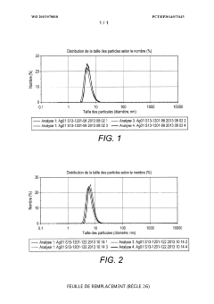
The synthesis of silver nanowires has been refined considerably, with polyol processes emerging as the dominant method. Current production techniques can yield nanowires with aspect ratios exceeding 1000 and diameters ranging from 20-100 nm. However, consistency in nanowire dimensions remains problematic at industrial scales, affecting the reproducibility of electrical and optical properties in printed films.
Formulation stability presents another significant challenge. Silver nanowires tend to aggregate and sediment in ink formulations, reducing shelf life and compromising print quality. While various stabilizing agents and surface modifications have been developed, achieving long-term stability without compromising conductivity remains difficult. Current commercial formulations typically offer stability periods of 6-12 months, which falls short of industry requirements for mass production scenarios.
Printing process compatibility continues to be a technical hurdle. Different printing methods—inkjet, screen, gravure, and flexographic printing—each impose specific rheological requirements on the ink. Current AgNW formulations often require customization for specific printing platforms, limiting their versatility. Viscosity control and prevention of nozzle clogging in inkjet systems remain particularly challenging due to the high aspect ratio of nanowires.
Post-processing requirements represent another constraint. Most AgNW inks require sintering at temperatures between 120-200°C to achieve optimal conductivity, which limits compatibility with heat-sensitive substrates. Alternative sintering methods such as photonic, plasma, and chemical sintering show promise but have not yet been widely implemented in industrial settings due to scalability concerns and equipment costs.
The environmental and health implications of AgNW technology also present challenges. Silver is classified as an environmental pollutant in many jurisdictions, and nanomaterials face increasing regulatory scrutiny. Current waste management protocols for production and end-of-life disposal remain underdeveloped, potentially limiting widespread adoption.
Cost factors continue to influence market penetration. Despite decreasing prices, silver nanowire inks remain 3-5 times more expensive than conventional silver flake alternatives on a per-unit-area basis. Production scaling has improved economics, but further cost reductions are necessary to compete with established technologies in price-sensitive applications.
Geographically, research leadership is distributed across regions, with North American institutions focusing on fundamental nanowire synthesis, European entities emphasizing environmentally sustainable formulations, and Asian manufacturers driving large-scale production efficiencies and application development.
Current Silver Nanowire Ink Formulation Solutions
01 Silver nanowire composition for enhanced conductivity
Silver nanowires can be formulated with specific compositions to enhance electrical conductivity in conductive inks. These compositions typically include silver nanowires with optimized dimensions (length and diameter), concentration, and dispersion agents. The formulation may also include additives that prevent aggregation and improve the uniform distribution of nanowires, resulting in conductive networks with lower resistance and higher conductivity.- Silver nanowire composition for enhanced conductivity: Silver nanowires can be formulated into conductive inks with specific compositions to enhance electrical conductivity. These formulations typically include silver nanowires with controlled dimensions (diameter and length), dispersing agents, and binders. The ratio of components and processing methods significantly impact the final conductivity of the printed patterns. Optimized compositions can achieve conductivity levels approaching that of bulk silver while maintaining flexibility and transparency.
- Surface treatment and modification of silver nanowires: Surface treatment and modification of silver nanowires can significantly improve their conductivity in conductive ink applications. Techniques include coating with conductive polymers, functionalization with specific chemical groups, and post-deposition treatments. These modifications enhance the contact between nanowires, reduce junction resistance, and protect against oxidation, resulting in improved electrical performance and stability of the conductive patterns.
- Processing techniques for silver nanowire conductive inks: Various processing techniques can be employed to enhance the conductivity of silver nanowire inks. These include sintering methods (photonic, thermal, plasma, or chemical), compression techniques, and specialized deposition processes. Post-processing treatments like annealing at specific temperatures can significantly reduce the resistance between nanowire junctions. These techniques enable the formation of highly conductive networks while maintaining the advantages of nanowire-based inks.
- Hybrid systems combining silver nanowires with other conductive materials: Hybrid conductive ink systems that combine silver nanowires with other conductive materials can achieve enhanced conductivity. These systems may incorporate graphene, carbon nanotubes, conductive polymers, or other metal nanoparticles. The synergistic effect between different conductive components can lead to improved electrical pathways, reduced contact resistance, and enhanced overall conductivity while potentially reducing the total silver content required.
- Substrate interaction and application-specific formulations: The interaction between silver nanowire conductive inks and various substrates plays a crucial role in determining final conductivity. Specialized formulations can be developed for specific substrates such as flexible polymers, paper, or textiles. Adhesion promoters, surface treatments, and customized rheological properties can optimize the ink-substrate interface, ensuring good wetting, adhesion, and electrical performance in applications ranging from flexible electronics to transparent conductive films.
02 Processing techniques for silver nanowire inks
Various processing techniques can significantly impact the conductivity of silver nanowire inks. These include sintering methods (photonic, thermal, plasma), coating processes (screen printing, inkjet printing, spray coating), and post-treatment procedures. Optimized processing parameters such as curing temperature, time, and pressure can reduce junction resistance between nanowires and improve overall conductivity of the printed patterns.Expand Specific Solutions03 Hybrid conductive systems with silver nanowires
Hybrid conductive systems that combine silver nanowires with other conductive materials can achieve enhanced conductivity. These systems may incorporate graphene, carbon nanotubes, conductive polymers, or other metal nanoparticles. The synergistic effect between different conductive components creates multiple conduction pathways, reducing overall resistance and improving conductivity while potentially reducing the amount of silver required.Expand Specific Solutions04 Surface modification of silver nanowires
Surface modification techniques can improve the conductivity of silver nanowire inks. These modifications include coating nanowires with conductive polymers, applying functional groups to improve dispersion, or creating core-shell structures. Modified surface properties can enhance the contact between nanowires, reduce oxidation, improve adhesion to substrates, and ultimately lead to higher conductivity in the final printed circuits.Expand Specific Solutions05 Substrate interaction and flexibility considerations
The interaction between silver nanowire inks and substrates plays a crucial role in determining conductivity. Formulations designed for specific substrates (flexible, stretchable, or rigid) include additives that improve adhesion and maintain conductivity under mechanical stress. For flexible electronics applications, special binders and elastomeric components help maintain conductive pathways when the substrate is bent or stretched, preserving electrical performance.Expand Specific Solutions
Leading Companies in Silver Nanowire Ink Development
The silver nanowire conductive ink market is in a growth phase, with increasing adoption in flexible electronics and printed circuit applications. The global market size is expanding rapidly, projected to reach significant value due to rising demand for touchscreens, wearables, and IoT devices. Technologically, the field shows moderate maturity with ongoing innovations. Key players include established chemical companies like Henkel AG and Daicel Corp alongside specialized innovators such as Genes'Ink, Poly-Ink, and Copprint Technologies. Academic-industry collaboration is evident with institutions like Industrial Technology Research Institute and Oregon State University partnering with companies like NthDegree Technologies and Shenzhen Huake Chuangzhi Technology to advance formulation techniques, printability, and conductivity performance while reducing production costs.
Genes'Ink SAS
Technical Solution: Genes'Ink has developed advanced silver nanowire (AgNW) conductive ink formulations specifically optimized for various printing technologies including inkjet, screen, and flexographic printing. Their proprietary technology focuses on creating stable dispersions of high-aspect-ratio silver nanowires in customized solvent systems that maintain conductivity while enabling excellent printability. The company's AgNW inks feature nanowires with diameters of 30-50 nm and lengths of 10-20 μm, creating highly conductive networks at lower silver loadings compared to conventional silver flake inks. Their formulations incorporate specialized additives that prevent nanowire aggregation during the printing process and promote strong adhesion to various substrates including PET, glass, and paper. Genes'Ink has also developed post-processing techniques that require significantly lower sintering temperatures (80-120°C) than traditional silver inks, making them compatible with heat-sensitive flexible substrates.
Strengths: Superior conductivity at lower silver content (reducing material costs), compatibility with flexible substrates, and lower sintering temperatures enabling use on heat-sensitive materials. Weaknesses: Higher cost compared to carbon-based alternatives, potential for oxidation in harsh environments without proper encapsulation, and more complex formulation requirements to maintain nanowire dispersion stability.
PARU Co., Ltd.
Technical Solution: PARU has developed specialized silver nanowire conductive inks that leverage their expertise in nanomaterial synthesis and formulation. Their technology centers on ultra-long silver nanowires (lengths exceeding 25 μm) with precisely controlled diameters (20-30 nm), creating highly efficient conductive networks with minimal junction resistance. PARU's proprietary synthesis method produces nanowires with pentagonal cross-sections that enhance mechanical stability and electrical performance. Their ink formulations incorporate custom-developed dispersants that prevent nanowire agglomeration while maintaining long-term suspension stability, addressing a key challenge in nanowire ink development. The company has pioneered a unique surface modification technique that enhances nanowire-to-nanowire contact, reducing junction resistance by up to 40% compared to untreated nanowires. PARU's inks are compatible with various printing methods including screen, gravure, and slot-die coating, achieving sheet resistances below 20 Ω/sq at optical transparencies exceeding 90%. Their formulations also feature specialized additives that enhance environmental stability, protecting the nanowires from oxidation and sulfidation in challenging operating conditions.
Strengths: Exceptional conductivity-to-transparency ratio ideal for transparent electrode applications, superior mechanical flexibility with minimal conductivity loss after repeated bending cycles, and excellent batch-to-batch consistency. Weaknesses: Higher production costs due to specialized nanowire synthesis requirements, more limited shelf life compared to conventional silver particle inks, and greater sensitivity to processing conditions during printing and curing.
Key Patents and Innovations in Nanowire Conductivity
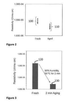
Method of Fabricating Highly Conductive Features with Silver Nanoparticle Ink at Low Temperature
PatentInactiveUS20170238425A1
Innovation
- A method involving silver nanoparticle inks applied to plastic substrates, annealed at low temperatures (up to 120°C), and then treated in a humidified atmosphere to reduce resistivity by at least a factor of 2, using hygroscopic capping agents like polyvinylpyrrolidone, which are partially removed to enhance particle contact and conductivity.
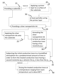
Ink comprising silver nanoparticles
PatentWO2015078818A1
Innovation
- A stable silver nanoparticle ink formulation comprising silver nanoparticles, a solvent, and specific rheology modifiers and dispersing agents, optimized for screen printing, which allows for improved stability and conductivity at lower annealing temperatures.
Environmental Impact and Sustainability Considerations
The environmental impact of silver nanowire (AgNW) conductive inks represents a critical consideration in their advancement and widespread adoption. Traditional electronic manufacturing processes often involve hazardous chemicals and significant energy consumption, making sustainability a growing concern in the industry. Silver nanowire inks offer several environmental advantages over conventional conductive materials, particularly when compared to indium tin oxide (ITO), which requires energy-intensive vacuum deposition processes and relies on scarce indium resources.
Despite these comparative benefits, silver nanowire production still presents notable environmental challenges. The synthesis of AgNWs typically involves polyol processes using chemicals such as ethylene glycol, polyvinylpyrrolidone (PVP), and silver nitrate, which can generate hazardous waste streams if not properly managed. Additionally, the mining and processing of silver itself carries significant environmental footprints, including habitat disruption, water pollution, and high energy consumption.
Recent research has focused on developing more sustainable approaches to AgNW ink production. Green synthesis methods utilizing plant extracts or environmentally benign reducing agents have shown promise in reducing toxic chemical usage. Several research groups have successfully demonstrated the production of silver nanowires using biologically derived materials as reducing and capping agents, significantly decreasing the environmental impact of the synthesis process.
End-of-life considerations represent another crucial aspect of environmental assessment. The recovery and recycling of silver from printed electronics remain technically challenging but economically attractive due to silver's inherent value. Emerging technologies for the selective recovery of silver from electronic waste show potential for creating closed-loop material systems, though these processes require further development for commercial viability.
Life cycle assessment (LCA) studies comparing silver nanowire inks to alternative conductive materials have yielded mixed results. While AgNW inks generally demonstrate lower energy requirements during application compared to vacuum-deposited alternatives, the upstream environmental impacts of silver mining and processing can offset these advantages. The environmental performance ultimately depends on factors including ink formulation, printing process efficiency, substrate material, and end-of-life management strategies.
Industry stakeholders are increasingly implementing sustainability initiatives, with several manufacturers developing water-based AgNW ink formulations that eliminate the need for harmful organic solvents. Additionally, efforts to reduce silver content through optimized nanowire morphologies and hybrid conductive systems are advancing, potentially decreasing resource intensity while maintaining performance characteristics. These developments align with broader electronic industry trends toward more environmentally responsible manufacturing practices.
Manufacturing Scalability and Cost Analysis
The manufacturing scalability of silver nanowire (AgNW) conductive inks represents a critical factor in their commercial viability. Current production methods have evolved significantly, with solution-phase synthesis approaches demonstrating promising scalability potential. Large-scale production facilities can now achieve monthly outputs of 50-100kg of high-quality silver nanowires, representing a substantial improvement from laboratory-scale production of just a few years ago.
Cost analysis reveals that material expenses remain the primary economic barrier, with silver accounting for approximately 65-75% of the total production cost. Recent innovations in synthesis efficiency have reduced silver waste during manufacturing by nearly 30%, significantly improving cost structures. Additionally, advances in polyol processes have decreased reaction times from 4-6 hours to under 2 hours in optimized production environments, enhancing throughput capabilities.
Production yield rates have improved from 70-80% to consistently above 90% in state-of-the-art facilities, further enhancing economic viability. The development of continuous flow reactors, replacing batch processing methods, has demonstrated capacity increases of 3-5 times while maintaining nanowire quality and dimensional consistency. These advancements have contributed to a gradual price reduction of approximately 15-20% annually over the past three years.
Equipment investment requirements present another significant consideration. Modern AgNW production lines require specialized filtration systems, precise temperature control mechanisms, and advanced purification equipment. Initial capital expenditure for a mid-scale production facility typically ranges from $2-5 million, with ROI periods of 3-4 years at current market demand levels.
Environmental and regulatory compliance adds complexity to manufacturing scale-up. Silver recovery systems now achieve 85-95% reclamation rates, addressing both economic and environmental concerns. Water usage has been reduced by implementing closed-loop systems that recycle up to 80% of process water. These sustainability improvements have reduced regulatory compliance costs by approximately 25% compared to earlier production methods.
When comparing AgNW inks to alternative conductive materials, manufacturing economics increasingly favor nanowire solutions. Production costs for AgNW inks have decreased to $8-12 per gram (depending on specifications), approaching cost competitiveness with traditional ITO alternatives when considering total application costs. Market analysis indicates that achieving price points below $5 per gram would trigger widespread adoption across multiple industries, a threshold that appears achievable within the next 3-5 years based on current cost reduction trajectories.
Unlock deeper insights with Patsnap Eureka Quick Research — get a full tech report to explore trends and direct your research. Try now!
Generate Your Research Report Instantly with AI Agent
Supercharge your innovation with Patsnap Eureka AI Agent Platform!