Comparative Study of Silver Nanowire and ITO Films
SEP 25, 20259 MIN READ
Generate Your Research Report Instantly with AI Agent
Patsnap Eureka helps you evaluate technical feasibility & market potential.
Silver Nanowire and ITO Films Background and Objectives
Transparent conductive films (TCFs) have been a cornerstone technology in modern optoelectronic devices, with Indium Tin Oxide (ITO) serving as the industry standard for decades. However, the scarcity of indium resources, coupled with the inherent brittleness of ITO films, has prompted researchers to explore alternative materials. Silver nanowires (AgNWs) have emerged as a promising candidate due to their excellent electrical conductivity, optical transparency, and mechanical flexibility.
The evolution of TCF technology can be traced back to the 1970s when ITO was first commercialized for display applications. ITO quickly became the dominant material due to its balanced performance in transparency and conductivity. By the early 2000s, with the proliferation of touch screens and flexible electronics, the limitations of ITO became increasingly apparent, catalyzing research into alternative materials including carbon nanotubes, graphene, conductive polymers, and metallic nanowires.
Silver nanowires represent a significant technological advancement in this field. First synthesized through the polyol process in the early 2000s, AgNWs have rapidly progressed from laboratory curiosities to commercially viable alternatives. Their development has been accelerated by innovations in synthesis methods, deposition techniques, and post-treatment processes that enhance their performance characteristics.
The current technological trajectory suggests a gradual transition from ITO to AgNW-based TCFs in specific application domains, particularly those requiring mechanical flexibility or formed on non-planar surfaces. This transition is driven by both technical advantages and economic considerations, as the price volatility of indium continues to pose challenges for manufacturers.
The primary technical objectives in this comparative study are to evaluate the performance metrics of AgNW films against ITO benchmarks across multiple parameters: sheet resistance, optical transmittance, haze factor, mechanical durability, environmental stability, and manufacturing scalability. Additionally, this study aims to identify application-specific advantages and limitations of each technology to guide strategic implementation decisions.
From a market perspective, this research seeks to assess the economic viability of AgNW technology as a direct replacement for ITO in existing applications and as an enabling technology for emerging flexible electronics markets. The cost structure analysis will consider raw material availability, processing requirements, and lifecycle considerations including recyclability and environmental impact.
The long-term objective is to develop a comprehensive technology roadmap that outlines the potential evolution of both ITO and AgNW technologies, identifying key inflection points where AgNWs may achieve performance or cost parity with ITO across different application segments. This roadmap will serve as a strategic planning tool for research prioritization and investment decisions in transparent conductive film technologies.
Market Analysis for Transparent Conductive Films
The transparent conductive film (TCF) market has experienced significant growth over the past decade, primarily driven by the expanding electronics industry and increasing demand for touch-enabled devices. Currently valued at approximately 5.1 billion USD in 2023, the market is projected to reach 8.7 billion USD by 2028, representing a compound annual growth rate (CAGR) of 11.3%. This growth trajectory is supported by the proliferation of smartphones, tablets, wearable devices, and emerging applications in automotive displays and smart home technologies.
Indium Tin Oxide (ITO) has traditionally dominated the TCF market, accounting for nearly 70% of market share due to its established manufacturing infrastructure and reliable performance characteristics. However, the market is witnessing a gradual shift toward alternative materials, with silver nanowire (AgNW) technology emerging as a promising contender. The AgNW segment is growing at a faster rate of approximately 17.5% annually, compared to ITO's more modest growth of 6.8%.
Regional analysis reveals that Asia-Pacific continues to be the manufacturing hub for TCFs, with China, South Korea, Japan, and Taiwan collectively accounting for over 65% of global production. North America and Europe represent significant consumption markets, particularly for premium applications requiring high-performance TCFs. The market in emerging economies is expanding rapidly, with India and Southeast Asian countries showing growth rates exceeding 15% annually.
End-use segmentation indicates that consumer electronics remains the largest application sector, consuming approximately 58% of TCF production. However, emerging applications in photovoltaics (12%), automotive displays (9%), and smart architecture (7%) are diversifying the market landscape and creating new growth opportunities for both ITO and alternative technologies like AgNW.
Price sensitivity analysis reveals interesting market dynamics. While ITO films typically command prices ranging from $10-30 per square meter depending on quality and specifications, AgNW films are currently positioned in the $15-40 range. This price differential is gradually narrowing as AgNW manufacturing scales up and production efficiencies improve. Market forecasts suggest that by 2026, AgNW could achieve price parity with ITO for certain applications, potentially accelerating market adoption.
Customer preference surveys indicate growing interest in flexible display technologies, with 63% of OEMs expressing plans to incorporate flexible components in their product roadmaps within the next three years. This trend strongly favors AgNW technology due to its superior flexibility compared to the brittle nature of ITO films, suggesting a potential inflection point in market share dynamics as flexible display adoption accelerates.
Current Status and Technical Challenges
The global transparent conductive film market is currently dominated by indium tin oxide (ITO), which has been the industry standard for decades due to its excellent combination of optical transparency and electrical conductivity. However, the landscape is evolving rapidly as silver nanowire (AgNW) technology emerges as a viable alternative. Current market analysis indicates that while ITO still holds approximately 85-90% of the market share, AgNW films are experiencing a compound annual growth rate of over 20%, significantly outpacing the overall market growth.
In terms of technological development, ITO has reached a mature stage with well-established manufacturing processes and integration techniques. The current state-of-the-art ITO films achieve sheet resistances of 10-100 Ω/sq with optical transmittance exceeding 90% in the visible spectrum. However, ITO faces inherent limitations that present significant challenges for next-generation applications, particularly in flexible electronics.
The primary technical challenges for ITO include its inherent brittleness, which severely limits its application in flexible and stretchable devices. ITO films typically crack at strain levels as low as 2-3%, rendering them unsuitable for emerging form factors. Additionally, the indium supply chain poses sustainability concerns, as indium is classified as a critical raw material with limited global reserves and geographically concentrated production, primarily in China, South Korea, and Japan.
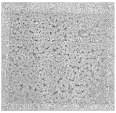
Silver nanowire technology, while promising, faces its own set of challenges. Current AgNW films demonstrate competitive performance with sheet resistances of 15-50 Ω/sq and optical transmittance of 88-95%. However, long-term stability remains a significant hurdle, with silver nanowires being susceptible to oxidation and sulfidation in ambient conditions. Junction resistance between individual nanowires also presents a fundamental limitation to achieving ultra-low sheet resistance values.
Manufacturing scalability represents another critical challenge for AgNW technology. While solution-based deposition methods offer potential cost advantages, achieving uniform performance across large-area substrates with high yield remains difficult. Current industrial production capabilities lag behind those of ITO, with fewer established suppliers and less standardized quality control protocols.
Geographically, research and development in these technologies show distinct patterns. ITO technology advancement is concentrated in East Asia, particularly Japan and South Korea, where major display manufacturers have established significant intellectual property portfolios. In contrast, AgNW innovation is more distributed, with significant contributions from North American startups and research institutions, European materials science centers, and emerging Chinese manufacturers focusing on cost-effective production methods.
In terms of technological development, ITO has reached a mature stage with well-established manufacturing processes and integration techniques. The current state-of-the-art ITO films achieve sheet resistances of 10-100 Ω/sq with optical transmittance exceeding 90% in the visible spectrum. However, ITO faces inherent limitations that present significant challenges for next-generation applications, particularly in flexible electronics.
The primary technical challenges for ITO include its inherent brittleness, which severely limits its application in flexible and stretchable devices. ITO films typically crack at strain levels as low as 2-3%, rendering them unsuitable for emerging form factors. Additionally, the indium supply chain poses sustainability concerns, as indium is classified as a critical raw material with limited global reserves and geographically concentrated production, primarily in China, South Korea, and Japan.
Silver nanowire technology, while promising, faces its own set of challenges. Current AgNW films demonstrate competitive performance with sheet resistances of 15-50 Ω/sq and optical transmittance of 88-95%. However, long-term stability remains a significant hurdle, with silver nanowires being susceptible to oxidation and sulfidation in ambient conditions. Junction resistance between individual nanowires also presents a fundamental limitation to achieving ultra-low sheet resistance values.
Manufacturing scalability represents another critical challenge for AgNW technology. While solution-based deposition methods offer potential cost advantages, achieving uniform performance across large-area substrates with high yield remains difficult. Current industrial production capabilities lag behind those of ITO, with fewer established suppliers and less standardized quality control protocols.
Geographically, research and development in these technologies show distinct patterns. ITO technology advancement is concentrated in East Asia, particularly Japan and South Korea, where major display manufacturers have established significant intellectual property portfolios. In contrast, AgNW innovation is more distributed, with significant contributions from North American startups and research institutions, European materials science centers, and emerging Chinese manufacturers focusing on cost-effective production methods.
Current Technical Solutions Comparison
01 Fabrication methods for silver nanowire and ITO composite films
Various methods for fabricating transparent conductive films that combine silver nanowires with indium tin oxide (ITO). These techniques include coating processes, embedding nanowires in ITO matrices, and hybrid deposition methods that optimize the electrical conductivity while maintaining high optical transparency. The composite structure leverages the high conductivity of silver nanowires with the stability and optical properties of ITO.- Fabrication methods for silver nanowire and ITO composite films: Various techniques for manufacturing composite films that combine silver nanowires with indium tin oxide (ITO) to create transparent conductive films. These methods include coating processes, deposition techniques, and patterning approaches that optimize the integration of these materials to achieve desired electrical and optical properties. The composite structure leverages the high conductivity of silver nanowires while maintaining the transparency advantages of ITO.
- Transparent electrode applications in display technology: Implementation of silver nanowire and ITO films as transparent electrodes in various display technologies including touchscreens, OLED displays, and LCD panels. These materials provide the necessary combination of high optical transparency and electrical conductivity required for modern display applications. The films enable the development of flexible, foldable, and high-performance display devices with improved touch sensitivity and visual clarity.
- Enhancement of electrical and optical properties: Methods for improving the performance characteristics of silver nanowire and ITO films, focusing on enhancing conductivity while maintaining high transparency. Techniques include optimizing nanowire density, improving junction resistance between nanowires, surface treatments, and developing hybrid structures. These enhancements result in films with lower sheet resistance, higher optical transmittance, and better mechanical durability for various electronic applications.
- Flexible and stretchable transparent conductive films: Development of flexible and stretchable transparent conductive films using silver nanowires and ITO combinations. These films maintain electrical conductivity under bending, folding, or stretching conditions, making them suitable for wearable electronics, flexible displays, and conformable touch sensors. Various substrate materials and embedding techniques are employed to achieve mechanical flexibility while preserving the electrical and optical properties of the conductive layers.
- Manufacturing processes for large-scale production: Industrial-scale manufacturing techniques for silver nanowire and ITO films, including roll-to-roll processing, spray coating, and other scalable deposition methods. These processes focus on achieving uniform film quality, reducing production costs, and enabling high-volume manufacturing. Innovations in process control, material handling, and quality assurance ensure consistent performance characteristics across large-area transparent conductive films for commercial applications.
02 Flexible transparent conductive films using silver nanowires
Development of flexible transparent conductive films using silver nanowires as alternatives to traditional ITO films. These films offer advantages in flexibility, stretchability, and mechanical durability while maintaining high electrical conductivity and optical transparency. Applications include flexible displays, touch panels, and wearable electronics where traditional rigid ITO films are unsuitable.Expand Specific Solutions03 Performance enhancement techniques for silver nanowire networks
Methods to enhance the performance of silver nanowire networks through post-treatment processes such as thermal annealing, chemical treatments, and junction welding. These techniques reduce contact resistance between nanowires, improve adhesion to substrates, and enhance long-term stability. The treatments result in transparent conductive films with improved conductivity, transparency, and environmental stability compared to untreated silver nanowire networks.Expand Specific Solutions04 Hybrid structures combining silver nanowires with other conductive materials
Development of hybrid transparent conductive structures that combine silver nanowires with other conductive materials such as graphene, carbon nanotubes, or conductive polymers. These hybrid structures leverage the complementary properties of different materials to achieve superior performance characteristics including lower sheet resistance, higher optical transparency, better mechanical flexibility, and improved environmental stability compared to single-material films.Expand Specific Solutions05 Applications of silver nanowire and ITO films in electronic devices
Implementation of silver nanowire and ITO films in various electronic devices including touch screens, solar cells, OLEDs, and electromagnetic interference shielding. The films serve as transparent electrodes that provide both electrical conductivity and optical transparency required for these applications. Device-specific optimizations include patterning techniques, integration methods, and interface engineering to enhance device performance and reliability.Expand Specific Solutions
Key Industry Players and Competition Landscape
The silver nanowire (AgNW) and ITO film market is currently in a growth phase, with increasing demand for transparent conductive films in touch panels, displays, and photovoltaics. The global market size is estimated at $5-7 billion, expanding at 8-10% CAGR. Technologically, AgNW films are gaining momentum as a viable alternative to traditional ITO, offering advantages in flexibility and cost. Leading players include C3 Nano with proprietary AgNW solutions, BOE Technology and LG Display as major display manufacturers integrating these technologies, while research institutions like KAIST and Duke University drive innovation. Established materials companies such as 3M, Merck Patent GmbH, and FUJIFILM are developing competitive formulations, indicating the technology's transition from emerging to mainstream status in transparent conductor applications.
3M Innovative Properties Co.
Technical Solution: 3M has developed an advanced silver nanowire transparent conductive film technology branded as "3M™ Flex Film" that offers a compelling alternative to ITO. Their approach utilizes a proprietary silver nanowire synthesis method that produces ultra-thin nanowires (diameter <20nm) with exceptional length-to-diameter ratios exceeding 1000:1. This unique morphology enables the formation of highly conductive networks at very low nanowire concentrations, resulting in superior optical transparency. 3M's manufacturing process incorporates specialized surface treatments that enhance adhesion to various substrate materials while maintaining flexibility. Their films achieve sheet resistance values of 20-30 ohms/sq with transparency above 92% in the visible spectrum. A key innovation in 3M's technology is their multi-layer coating architecture that encapsulates the silver nanowire network between protective layers, significantly improving environmental stability against oxidation and sulfidation. The company has also developed specialized patterning techniques that enable direct laser patterning of the conductive layer without damaging underlying substrates, simplifying the manufacturing process compared to traditional ITO etching.
Strengths: Exceptional durability with resistance to environmental degradation; excellent optical clarity with minimal haze; established global manufacturing infrastructure ensuring reliable supply chain. Weaknesses: Higher cost compared to some competing AgNW solutions; slightly higher sheet resistance than best-in-class alternatives; requires specialized handling during integration into some manufacturing processes.
Eastman Kodak Co.
Technical Solution: Kodak has developed an innovative hybrid transparent conductive film technology that combines silver nanowires with conductive polymers to create a cost-effective alternative to ITO. Their approach, called "Kodak Flexcon," utilizes a specialized silver nanowire synthesis process that produces nanowires with optimized aspect ratios (diameter 30-50nm, length 10-20μm) for balanced performance. Kodak's manufacturing technique involves a proprietary roll-to-roll coating process that enables high-throughput production while maintaining tight quality control. Their films achieve sheet resistance in the range of 30-50 ohms/sq with transparency of 88-92%. A key innovation in Kodak's technology is their conductive polymer matrix that surrounds the silver nanowire network, enhancing both mechanical stability and environmental protection. This hybrid structure improves adhesion to various substrates and reduces silver migration issues that can affect long-term reliability. Kodak has also developed specialized patterning techniques using photolithographic processes adapted from their imaging expertise, enabling precise patterning of conductive areas without damaging the nanowire network. Their solution has been successfully implemented in various touch sensor applications, demonstrating commercial viability.
Strengths: Excellent cost-performance ratio making it suitable for mid-range applications; good mechanical durability with resistance to cracking; established manufacturing processes leveraging Kodak's coating expertise. Weaknesses: Moderate sheet resistance limiting use in some high-performance applications; slightly lower transparency than premium AgNW solutions; potential for yellowing over extended exposure to UV light.
Core Patents and Technical Literature Analysis
Ink based on silver nanowires
PatentWO2023174772A1
Innovation
- Development of stable, transparent, and conductive ink formulations based on silver nanowires, suitable for additive manufacturing by screen printing, which replace ITO by using a combination of silver nanowires, monohydric alcohols, hydroxy propyl methylcellulose, ethylene glycol, and propylene glycol propyl ether, optimizing viscosity and composition to prevent foam formation and enhance conductivity.
Manufacturing Process and Scalability Assessment
The manufacturing processes for silver nanowire (AgNW) and indium tin oxide (ITO) films differ significantly, with important implications for scalability and commercial viability. ITO films are typically produced through vacuum-based physical vapor deposition methods, primarily sputtering. This process requires sophisticated equipment, high temperatures (often exceeding 300°C), and substantial energy consumption. The vacuum requirements and high-temperature processing limit throughput and increase production costs, though decades of industrial refinement have established reliable manufacturing protocols.
In contrast, AgNW films can be fabricated using solution-based processes including spin-coating, spray coating, rod coating, and roll-to-roll printing. These methods operate at lower temperatures (often below 150°C) and under ambient pressure conditions, significantly reducing energy requirements and equipment complexity. The solution-processability of AgNWs enables compatibility with flexible substrates that cannot withstand high-temperature ITO deposition processes.
Scale-up assessment reveals distinct advantages for AgNW technology. The roll-to-roll compatibility of AgNW deposition methods allows for continuous production with higher throughput than batch-processed ITO. Production rates for solution-processed AgNW films can exceed 100 m²/min, whereas ITO sputtering typically achieves only 5-10 m²/min. This throughput difference translates to potential cost reductions of 30-50% for large-area applications.
Material supply considerations also favor AgNWs for long-term scalability. Indium is classified as a critical raw material with limited global reserves, primarily sourced from zinc mining byproducts. Current estimates suggest indium supplies may face constraints within 20-30 years at current consumption rates. Silver, while also precious, has more established supply chains and approximately 5-7 times greater global reserves than indium.
Manufacturing yield analysis indicates that ITO processes have matured to achieve 85-90% yields in commercial production. AgNW processes currently demonstrate 75-85% yields but show rapid improvement trajectories as manufacturing techniques evolve. The primary yield challenges for AgNWs relate to dispersion stability and network uniformity across large areas.
Environmental impact assessments reveal that AgNW production generates approximately 35-45% lower carbon emissions compared to ITO manufacturing, primarily due to reduced energy requirements and elimination of vacuum processing. Water consumption is also significantly lower for AgNW production, though silver recovery systems are essential to prevent environmental contamination from production waste.
Environmental Impact and Sustainability Considerations
The environmental impact of transparent conductive films (TCFs) has become increasingly important as electronics manufacturing scales globally. Silver nanowire (AgNW) films present a compelling alternative to indium tin oxide (ITO) when considering ecological footprints. ITO production relies heavily on indium, a scarce element with limited global reserves primarily concentrated in China, Korea, and Canada. Mining and refining processes for indium are energy-intensive and generate significant waste, including toxic byproducts that can contaminate soil and water systems if not properly managed.
In contrast, silver nanowire production demonstrates lower energy requirements during manufacturing. While silver mining does have environmental consequences, the amount of silver needed for nanowire films is substantially less than the indium required for comparable ITO applications. Recent life cycle assessments indicate that AgNW films can reduce carbon emissions by approximately 30-45% compared to traditional ITO manufacturing processes, primarily due to lower temperature requirements during deposition and patterning.
Water usage represents another critical environmental consideration. ITO production typically consumes 1.5-2 times more water than AgNW manufacturing for equivalent functional units. Additionally, waste management challenges differ significantly between these technologies. ITO etching processes generate acidic waste streams containing heavy metals, whereas AgNW production primarily produces organic solvent waste which, while still requiring proper disposal, presents fewer long-term environmental hazards.
Recyclability further distinguishes these materials. ITO-coated substrates present significant challenges for end-of-life recycling due to the difficulty in separating the indium and tin from the substrate. Silver nanowires offer improved recoverability potential, with emerging technologies demonstrating up to 80% silver recovery from end-of-life devices. This recyclability aspect becomes increasingly important as electronic waste volumes continue to grow globally.
Energy efficiency during device operation also factors into sustainability considerations. Devices utilizing AgNW films typically demonstrate 5-10% lower power consumption compared to ITO-based alternatives due to lower sheet resistance at equivalent transparency. This operational efficiency translates to reduced lifetime carbon footprints for consumer electronics and touch displays.
Looking forward, sustainability certifications and regulatory compliance will likely favor AgNW technology as environmental standards become more stringent. Several major electronics manufacturers have already begun transitioning to silver nanowire technology, citing both performance advantages and environmental responsibility commitments in their sustainability reports. This shift signals a growing recognition of the importance of considering full lifecycle environmental impacts in materials selection for next-generation electronic devices.
Unlock deeper insights with Patsnap Eureka Quick Research — get a full tech report to explore trends and direct your research. Try now!
Generate Your Research Report Instantly with AI Agent
Supercharge your innovation with Patsnap Eureka AI Agent Platform!