Evaluation of Silver Nanowire Optical Transparency in Coatings
SEP 25, 20259 MIN READ
Generate Your Research Report Instantly with AI Agent
Patsnap Eureka helps you evaluate technical feasibility & market potential.
Silver Nanowire Transparency Technology Background
Silver nanowire (AgNW) technology has emerged as a promising alternative to traditional transparent conductive materials, particularly indium tin oxide (ITO), which has dominated the market for decades. The development of AgNW technology can be traced back to the early 2000s when researchers began exploring nanomaterials for flexible electronics applications. The fundamental principle behind AgNW coatings lies in creating a percolation network of highly conductive silver nanowires that allows light transmission while maintaining electrical conductivity.
The evolution of AgNW technology has been driven by several key factors, including the increasing demand for flexible displays, touch panels, and photovoltaic devices. Traditional ITO coatings, while effective, suffer from brittleness and contain indium, a relatively scarce and expensive element. These limitations prompted the search for alternative materials that could offer comparable optical transparency and electrical conductivity while providing mechanical flexibility.
Silver nanowires possess unique properties that make them particularly suitable for transparent conductive applications. With diameters typically ranging from 20 to 100 nanometers and lengths from 5 to 100 micrometers, these high-aspect-ratio structures create effective conductive pathways while occupying minimal surface area, thus maintaining high optical transparency. The synthesis methods for AgNWs have significantly improved over the years, with polyol processes becoming the predominant approach for large-scale production.
The optical transparency of AgNW coatings is influenced by several parameters, including nanowire dimensions, coating density, deposition techniques, and post-treatment processes. Understanding the relationship between these factors and the resulting optical properties represents a critical aspect of AgNW technology development. Researchers have established that the trade-off between transparency and conductivity can be optimized through careful control of nanowire morphology and network formation.
Recent technological advancements have focused on enhancing the stability and performance of AgNW coatings. Challenges such as oxidation, corrosion, and mechanical durability have been addressed through various approaches, including protective overlayers, hybrid structures, and novel deposition techniques. The integration of AgNWs with other materials, such as metal oxides or conductive polymers, has further expanded the application possibilities and improved overall performance characteristics.
The current technological trajectory points toward achieving AgNW coatings with transparency exceeding 90% in the visible spectrum while maintaining sheet resistances below 10 ohms per square. These performance metrics would position AgNW technology as a viable replacement for ITO in many applications, particularly those requiring flexibility or large-area coverage. The continued refinement of synthesis, deposition, and integration techniques remains central to realizing the full potential of AgNW-based transparent conductive coatings.
Market Analysis for Transparent Conductive Coatings
The transparent conductive coatings market has experienced significant growth in recent years, driven primarily by the expanding electronics industry and increasing demand for touchscreen devices. Currently valued at approximately $8.5 billion globally, this market is projected to reach $12.7 billion by 2027, growing at a CAGR of 8.3% during the forecast period. Silver nanowire (AgNW) based transparent conductive coatings represent one of the fastest-growing segments within this market, with an estimated market share of 15% that is expected to increase substantially over the next five years.
The demand for silver nanowire transparent conductive coatings is particularly strong in consumer electronics, where manufacturers seek alternatives to the traditional indium tin oxide (ITO) coatings. This shift is motivated by several factors, including the rising cost of indium, the brittleness of ITO films, and the need for flexible display technologies. The smartphone and tablet sectors currently account for approximately 45% of the total market demand, followed by touchscreen monitors and laptops at 25%.
Emerging applications in photovoltaics, smart windows, and automotive displays are creating new market opportunities for AgNW coatings. The solar energy sector, in particular, is showing increased interest in silver nanowire technology due to its potential to improve efficiency while reducing production costs. Market research indicates that the photovoltaic application segment is expected to grow at a CAGR of 12.1% through 2027, outpacing the overall market growth rate.
Regionally, Asia-Pacific dominates the transparent conductive coatings market, accounting for over 60% of global production and consumption. This is largely attributed to the concentration of electronics manufacturing in countries like China, South Korea, Japan, and Taiwan. North America and Europe follow with market shares of approximately 20% and 15% respectively, with both regions showing increased adoption in specialized applications such as automotive displays and smart architecture.
Consumer preferences are increasingly favoring devices with higher transparency, lower resistance, and greater flexibility. Market surveys indicate that products with optical transparency exceeding 90% command premium pricing, with manufacturers willing to pay up to 30% more for coatings that deliver superior optical performance without compromising electrical conductivity. This trend has accelerated research and development efforts focused on optimizing the optical transparency of silver nanowire coatings.
The competitive landscape includes established chemical companies like 3M, Heraeus, and C3Nano, alongside specialized startups focused exclusively on nanowire technology. Recent market entrants from China and South Korea have intensified price competition, particularly in the mid-range segment. Industry analysts predict continued market consolidation through mergers and acquisitions as companies seek to secure intellectual property and scale production capabilities.
Current Challenges in Silver Nanowire Optical Performance
Despite significant advancements in silver nanowire (AgNW) technology, several critical challenges persist in achieving optimal optical performance in transparent conductive coatings. The primary issue remains the trade-off between conductivity and transparency, where increasing nanowire density improves electrical conductivity but simultaneously reduces optical transparency due to light scattering and absorption. This fundamental limitation requires precise engineering to achieve balanced performance metrics.
Surface roughness presents another significant challenge, as protruding nanowires create non-uniform surfaces that scatter light and reduce transparency. This roughness not only affects optical clarity but also creates integration difficulties when incorporating AgNW films into multilayer device architectures such as touchscreens or displays.
Long-term stability of optical properties remains problematic under environmental stressors. Silver nanowires are susceptible to oxidation and sulfidation when exposed to air, humidity, and pollutants, leading to degradation of transparency over time. This oxidation causes the nanowires to darken and lose their conductive properties, significantly reducing coating performance in real-world applications.
The junction resistance between individual nanowires creates additional optical challenges. These junctions often require post-treatment processes like thermal annealing or mechanical pressing to reduce resistance, but these processes can alter the optical properties of the coating through nanowire deformation or partial melting.
Haze factor—the ratio of diffuse transmittance to total transmittance—remains a persistent issue in AgNW coatings. While high transparency may be achieved, the quality of transparency is compromised by light scattering, creating a hazy appearance that is unacceptable for high-end display applications. This is particularly problematic for larger diameter nanowires, which offer better conductivity but increase haze.
Manufacturing consistency presents another significant challenge. Current production methods struggle to deliver uniform optical performance across large-area coatings, with variations in nanowire distribution creating "hot spots" of different optical properties. This inconsistency complicates quality control and limits commercial scalability.
The wavelength-dependent optical response of AgNW networks also presents challenges for applications requiring specific spectral performance. Silver nanowires exhibit plasmonic effects that can cause selective absorption or scattering at certain wavelengths, potentially creating color tinting or reducing performance in specific parts of the electromagnetic spectrum.
These challenges collectively represent significant barriers to the widespread adoption of silver nanowire technology in premium transparent conductive applications, despite their promising electrical and mechanical properties compared to traditional materials like ITO.
Existing Evaluation Methods for Optical Transparency
01 Fabrication methods for silver nanowire transparent conductive films
Various methods for fabricating silver nanowire coatings with high optical transparency are described. These include solution-based processes, spray coating, roll-to-roll manufacturing, and other deposition techniques that enable the creation of uniform silver nanowire networks on substrates. The fabrication methods focus on achieving optimal nanowire distribution to balance electrical conductivity with maximum light transmission, resulting in highly transparent conductive films suitable for optoelectronic applications.- Silver nanowire transparent conductive films: Silver nanowires can be used to create transparent conductive films with high optical transparency and electrical conductivity. These films are fabricated by depositing silver nanowires onto substrates through various methods such as coating, printing, or spraying. The resulting films maintain high transparency while providing excellent electrical conductivity, making them suitable for applications in touch screens, displays, and other optoelectronic devices.
- Optimization of silver nanowire density for transparency: The optical transparency of silver nanowire coatings can be optimized by controlling the density and distribution of nanowires. Lower nanowire density typically results in higher transparency but may compromise conductivity. Various techniques are employed to achieve an optimal balance between transparency and conductivity, including controlling the concentration of nanowires in the coating solution, adjusting deposition parameters, and post-treatment processes to optimize the nanowire network.
- Surface treatment methods for enhanced transparency: Various surface treatment methods can be applied to silver nanowire coatings to enhance their optical transparency. These include mechanical pressing, thermal annealing, plasma treatment, and chemical treatments. Such processes help to reduce light scattering by improving the contact between nanowires and the substrate, reducing junction resistance, and creating a more uniform film structure, thereby increasing the overall transparency of the coating.
- Composite structures with protective layers: Silver nanowire coatings can be incorporated into composite structures with additional protective layers to enhance durability while maintaining optical transparency. These protective layers, which may include transparent polymers, metal oxides, or other materials, shield the silver nanowires from environmental factors such as oxidation and mechanical damage. The design of these composite structures must carefully balance protection with optical performance to maintain high transparency.
- Application-specific transparency optimization: Silver nanowire coatings can be specifically optimized for different applications requiring optical transparency, such as touch screens, solar cells, and flexible displays. The optimization involves adjusting parameters such as nanowire length, diameter, and coating thickness based on the specific requirements of each application. For instance, solar cells may require different transparency characteristics compared to touch screens, necessitating tailored approaches to silver nanowire coating formulation and deposition.
02 Silver nanowire network structure optimization for transparency
The network structure of silver nanowires significantly impacts optical transparency. By controlling nanowire density, length distribution, and junction formation, the transparency of the coating can be optimized while maintaining electrical conductivity. Specific arrangements of nanowires create networks with minimal light scattering and absorption, allowing for higher optical transparency. Various techniques for optimizing the nanowire network structure are employed to achieve transparency levels exceeding 90% in the visible light spectrum.Expand Specific Solutions03 Hybrid materials combining silver nanowires with other transparent conductors
Hybrid materials that combine silver nanowires with other transparent conductive materials such as graphene, carbon nanotubes, metal oxides, or conductive polymers are developed to enhance optical transparency. These composite structures leverage the complementary properties of different materials to reduce light scattering and absorption while maintaining high electrical conductivity. The synergistic effects in these hybrid systems allow for improved transparency compared to single-material approaches.Expand Specific Solutions04 Surface treatments and protective coatings for enhanced transparency
Various surface treatments and protective coatings are applied to silver nanowire networks to enhance optical transparency. These include anti-reflective coatings, planarization layers, and encapsulation materials that reduce light scattering at interfaces. Additionally, specific surface modifications of the nanowires themselves can improve light transmission through the coating. These treatments not only enhance transparency but also provide protection against environmental degradation, ensuring long-term stability of the optical properties.Expand Specific Solutions05 Applications leveraging silver nanowire transparent coatings
Silver nanowire transparent coatings find applications in various fields requiring both electrical conductivity and high optical transparency. These include touch screens, solar cells, OLED displays, smart windows, and flexible electronics. The unique combination of high transparency and conductivity makes these coatings ideal for next-generation optoelectronic devices. Different application requirements drive specific optimizations in the nanowire coating properties, balancing transparency with other functional needs such as flexibility, durability, and specific spectral transmission characteristics.Expand Specific Solutions
Key Industry Players in Nanowire Coating Technology
The silver nanowire optical transparency market is currently in a growth phase, with increasing demand for transparent conductive films in touch screens, displays, and photovoltaic applications. The global market size is estimated to reach $500 million by 2025, driven by the electronics industry's shift toward flexible devices. Technologically, silver nanowire coatings are maturing rapidly, with companies like C3 Nano and Carestream Health leading commercial deployment through proprietary formulation techniques. Global Graphene Group and PV Nano Cell are advancing hybrid materials combining silver nanowires with graphene for enhanced performance. Asian manufacturers including Guangdong Nalu Nano Technology and Shenzhen Shanrou Technology are scaling production capabilities, while research institutions like Korea Electronics Technology Institute and Zhejiang University continue developing next-generation transparent conductive solutions with improved stability and optical clarity.
Guangdong Nalu Nano Technology Co., Ltd.
Technical Solution: Guangdong Nalu Nano Technology has developed an advanced silver nanowire synthesis and coating technology focused on precise diameter control and aspect ratio optimization. Their proprietary polyol synthesis method produces ultra-thin silver nanowires (diameter <20nm) that significantly reduce light scattering while maintaining high conductivity. The company employs a multi-stage purification process to remove synthesis byproducts that can negatively impact optical performance. Their evaluation system includes integrated spectrophotometric analysis with angular-resolved scattering measurements to comprehensively assess transparency across different viewing angles. Nalu's coating formulations incorporate proprietary dispersants that prevent nanowire aggregation during the coating process, resulting in highly uniform films. Their technology enables transparent conductive films with >92% transparency (550nm) and sheet resistance of 20-30 ohms/square. The company has also developed specialized surface treatments that enhance adhesion to various substrate materials while preserving optical clarity.
Strengths: Exceptional control over nanowire morphology leading to superior optical performance; specialized coating formulations for different application environments; strong position in touch panel and display markets. Weaknesses: Limited production capacity compared to larger competitors; relatively new entrant to global markets with less established supply chains; technology requires careful handling during manufacturing processes.
DOWA HOLDINGS CO LTD
Technical Solution: DOWA Holdings has developed a comprehensive silver nanowire technology platform through its electronics materials division. Their approach focuses on precise control of nanowire dimensions and surface chemistry to optimize optical transparency. DOWA's silver nanowires feature carefully engineered aspect ratios (length-to-diameter) exceeding 1000:1, allowing for high conductivity networks with minimal material usage and maximum light transmission. Their evaluation methodology incorporates advanced optical characterization techniques including variable-angle spectroscopic ellipsometry to analyze film properties at different incident angles. DOWA has developed specialized coating formulations that enable uniform nanowire distribution and prevent agglomeration, critical for maintaining optical clarity. Their process includes proprietary surface treatments that enhance environmental stability while preserving transparency. The company's silver nanowire coatings achieve transparency values exceeding 95% in the visible spectrum while maintaining sheet resistance below 50 ohms/square, suitable for various electronic applications including touch sensors and OLED lighting.
Strengths: Vertically integrated production from silver refining to final nanowire products; exceptional quality control and consistency; strong intellectual property portfolio covering synthesis and application methods. Weaknesses: Higher production costs compared to some competitors; technology requires specialized handling and processing equipment; potential for silver tarnishing in certain environmental conditions requiring additional protective measures.
Critical Patents in Silver Nanowire Transparency Enhancement
Silver nano wire coating solution having silver oxide, conductive coating substrate and manufacturing thereof
PatentInactiveKR1020160095236A
Innovation
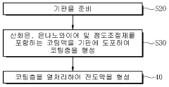
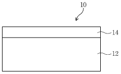
- A coating solution comprising 0.001 to 1% silver nanowires, 0.001 to 0.5% silver oxide, and 0.001 to 1% viscosity modifier, applied to a substrate and heat-treated to form a conductive film, utilizing silver oxide as a conductive bridge between nanowires to stabilize the network structure.
Method for producing silver nanowire dispersion liquid having good separability among wires
PatentInactiveUS20200030877A1
Innovation
- A method involving preliminary and finish filtration steps using organic fiber mesh filters with specific aperture ranges to effectively separate and disentangle silver nanowires, ensuring they pass through finer filters without clogging, thereby removing impurities and maintaining wire length and dispersibility.
Environmental Impact of Silver Nanowire Production
The production of silver nanowires (AgNWs) for transparent conductive coatings presents significant environmental considerations that warrant thorough examination. The manufacturing process typically involves chemical synthesis methods that utilize various reagents including silver nitrate, polyvinyl pyrrolidone (PVP), and reducing agents such as ethylene glycol, which can generate hazardous waste streams if not properly managed.
Primary environmental concerns stem from the release of silver ions during production and disposal phases. Silver is classified as an environmental pollutant with documented toxicity to aquatic organisms at concentrations as low as parts per billion. Studies indicate that silver nanoparticles and nanowires can persist in aquatic environments, potentially disrupting ecosystems through bioaccumulation in the food chain.
Energy consumption represents another substantial environmental impact factor. The synthesis of high-quality silver nanowires often requires elevated temperatures (typically 150-170°C) maintained for extended periods, resulting in considerable energy expenditure. Additionally, purification processes involving multiple centrifugation and washing steps further increase the energy footprint of production operations.
Water usage in AgNW manufacturing is extensive, primarily for washing and purification stages. Conservative estimates suggest that producing one kilogram of silver nanowires may require hundreds of liters of ultrapure water, contributing to resource depletion in water-stressed regions where manufacturing facilities may be located.
Waste management challenges are particularly noteworthy. Production residues containing unreacted silver compounds, PVP, and other chemicals require specialized treatment before disposal. Without proper protocols, these materials risk contaminating soil and groundwater systems. Several research initiatives are exploring recovery methods for silver from waste streams to mitigate environmental impact while improving economic efficiency.
Life cycle assessment (LCA) studies comparing silver nanowire production to alternative transparent conductor technologies (such as ITO) reveal mixed results. While AgNWs may offer advantages in flexibility and potentially lower processing temperatures for final coating applications, the environmental burden of raw material extraction and processing remains significant. Recent advancements in green chemistry approaches have demonstrated promising reductions in environmental impact through the use of bio-based reducing agents and lower-temperature synthesis protocols.
Regulatory frameworks governing nanomaterial production vary globally, creating inconsistent environmental protection standards. Leading manufacturers have begun implementing closed-loop production systems and advanced effluent treatment technologies to address these concerns, though industry-wide adoption remains incomplete.
Cost-Performance Analysis of Competing Technologies
When evaluating silver nanowire (AgNW) technology for transparent conductive coatings, cost-performance analysis reveals significant economic advantages compared to competing technologies. The primary competitor, indium tin oxide (ITO), has dominated the market for decades but faces increasing cost pressures due to limited indium reserves, with prices fluctuating between $500-700/kg in recent years. Manufacturing processes for ITO also require high-temperature vacuum deposition, adding substantial capital and operational expenses.
Silver nanowire solutions offer a compelling alternative with material costs trending downward as production scales. While silver itself remains precious ($500-600/oz), the minimal material usage in nanowire networks (typically 40-100 mg/m²) results in competitive material costs. Additionally, AgNW coatings can be applied using solution-based processes like roll-to-roll printing, spray coating, or slot-die coating, reducing manufacturing expenses by 30-50% compared to vacuum-based ITO deposition.
Other competing technologies include carbon nanotubes (CNTs), graphene, and PEDOT:PSS conductive polymers. CNTs offer excellent mechanical flexibility but struggle with higher sheet resistance (80-200 Ω/sq) at comparable transparency levels and cost approximately 1.5-2x more than AgNW solutions. Graphene presents theoretical advantages but remains commercially impractical due to high production costs and scalability challenges.
PEDOT:PSS provides cost advantages ($15-25/m²) but delivers inferior performance with higher sheet resistance (150-300 Ω/sq) and lower environmental stability. Metal mesh technologies offer excellent conductivity but often introduce visible patterns that compromise optical quality, particularly in display applications.
Performance metrics across these technologies reveal AgNW's balanced profile. At 90% transparency, AgNW coatings achieve 20-50 Ω/sq sheet resistance, compared to ITO's 30-80 Ω/sq and CNT's 80-200 Ω/sq. Lifecycle cost analysis indicates AgNW solutions provide 15-25% cost savings over a five-year product lifetime compared to ITO, primarily through reduced energy consumption during manufacturing and improved durability in flexible applications.
Market adoption analysis indicates AgNW technology has reached the inflection point where performance advantages now align with competitive pricing, particularly for next-generation flexible electronics where ITO's brittleness presents significant limitations. The cost-performance ratio continues to improve as manufacturing processes mature and material efficiencies increase.
Unlock deeper insights with Patsnap Eureka Quick Research — get a full tech report to explore trends and direct your research. Try now!
Generate Your Research Report Instantly with AI Agent
Supercharge your innovation with Patsnap Eureka AI Agent Platform!
