The Patent Landscape for Silver Nanowire in Haptics Technology
SEP 25, 20259 MIN READ
Generate Your Research Report Instantly with AI Agent
Patsnap Eureka helps you evaluate technical feasibility & market potential.
Silver Nanowire Haptics Background and Objectives
Silver nanowire (AgNW) technology has emerged as a revolutionary material in the field of haptics over the past decade. Initially developed for transparent conductive applications in displays, AgNWs have gradually transitioned into haptic technology due to their unique combination of electrical conductivity, mechanical flexibility, and optical transparency. The evolution of this technology can be traced from early research in nanomaterial synthesis in the early 2000s to the current integration in commercial haptic devices, marking a significant technological progression in human-machine interfaces.
The technological trajectory of AgNWs in haptics has been characterized by several key developments. First, the refinement of synthesis methods has enabled the production of high-aspect-ratio nanowires with controlled dimensions and improved conductivity. Second, integration techniques have evolved from simple film deposition to complex patterned structures that can detect and provide localized tactile feedback. Third, the coupling of AgNWs with other materials has created hybrid systems with enhanced durability and performance characteristics.
The primary objective of AgNW haptic technology is to create more intuitive, responsive, and immersive tactile interfaces. This includes developing thinner, more flexible haptic devices that can conform to curved surfaces, improving the spatial resolution of tactile feedback, reducing response time, and enhancing the range of tactile sensations that can be generated. Additionally, there is a focus on developing energy-efficient systems that can operate with minimal power consumption, which is crucial for portable and wearable applications.
Current research aims to overcome several technical challenges, including the long-term stability of AgNW networks under mechanical stress, the development of manufacturing processes suitable for large-scale production, and the integration of AgNW-based haptic systems with existing electronic platforms. The goal is to create haptic interfaces that not only provide realistic tactile feedback but also maintain performance over extended periods of use.
The potential applications of AgNW haptic technology span multiple sectors, including consumer electronics, healthcare, automotive, and virtual reality. In consumer electronics, the technology promises to enhance user interaction with touchscreens and wearable devices. In healthcare, it could enable more realistic surgical simulators and rehabilitation tools. In automotive settings, it may improve driver interfaces and safety systems. In virtual reality, AgNW-based haptics could significantly enhance immersion by providing realistic tactile feedback that complements visual and auditory stimuli.
As we look toward the future, the continued development of AgNW haptic technology is expected to play a crucial role in the evolution of human-computer interaction, potentially transforming how we perceive and interact with digital environments.
Market Demand Analysis for Haptic Feedback Solutions
The haptic feedback technology market is experiencing significant growth, driven by increasing demand for immersive user experiences across multiple industries. Current market analysis indicates that the global haptic technology market is projected to reach $4.8 billion by 2026, with a compound annual growth rate of 12.0% from 2021. This growth trajectory is particularly relevant for silver nanowire-based haptic solutions, which are gaining traction due to their superior performance characteristics.
Consumer electronics remains the dominant sector for haptic feedback applications, accounting for approximately 40% of the total market share. Smartphones, tablets, and wearable devices are primary drivers, with manufacturers increasingly incorporating advanced haptic feedback to differentiate their products in competitive markets. The gaming and virtual reality segments follow closely, where realistic tactile feedback significantly enhances user immersion and experience quality.
Automotive applications represent a rapidly expanding market for haptic technology, growing at 15.2% annually. Touch-based control systems in vehicles are transitioning from basic vibration feedback to more sophisticated haptic responses, creating opportunities for advanced materials like silver nanowires that can deliver precise, localized feedback while maintaining durability in automotive environments.
Healthcare applications are emerging as a promising growth sector, particularly in surgical simulation, rehabilitation systems, and remote medical procedures. The market for medical haptic devices is expected to grow at 14.5% annually through 2026, with increasing demand for training systems that can accurately simulate tissue resistance and texture.
Consumer preference surveys indicate strong market pull for more refined haptic experiences. Approximately 78% of smartphone users consider haptic feedback an important feature in their purchasing decisions, while 65% express dissatisfaction with current haptic solutions' precision and responsiveness. This gap between consumer expectations and existing technology capabilities presents a significant market opportunity for silver nanowire-based solutions that offer improved response times and tactile fidelity.
Industrial analysis reveals a shift toward thinner, more flexible display technologies incorporating haptic feedback, with projected market growth of 18% annually in this specific segment. Silver nanowire technology is particularly well-positioned to address this trend due to its inherent flexibility, transparency, and conductivity properties that enable seamless integration with next-generation display technologies.
Regional market assessment shows Asia-Pacific leading in haptic technology adoption, accounting for 42% of global market share, followed by North America (28%) and Europe (22%). Emerging markets in Latin America and Africa are showing accelerated growth rates as smartphone penetration increases and manufacturing capabilities expand in these regions.
Silver Nanowire Haptics: Current State and Challenges
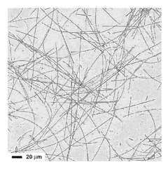
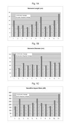
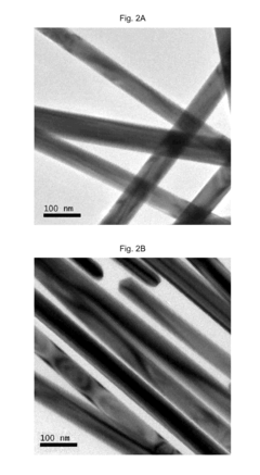
Silver nanowire (AgNW) technology represents a significant advancement in haptic feedback systems, yet faces several critical challenges that impede its widespread adoption. Currently, AgNW networks demonstrate exceptional electrical conductivity and mechanical flexibility, making them ideal candidates for next-generation haptic interfaces. These nanowires, typically 30-100 nm in diameter and several micrometers in length, can be integrated into transparent, stretchable substrates to create responsive tactile surfaces that maintain functionality under deformation.
The primary technical challenge confronting AgNW haptic systems is durability under repeated mechanical stress. Current implementations show performance degradation after approximately 10,000-15,000 bending cycles, significantly below the industry standard requirement of 100,000+ cycles for consumer electronics. This limitation stems from nanowire junction failures and silver oxidation processes that progressively increase electrical resistance and diminish haptic response fidelity.
Manufacturing scalability presents another substantial hurdle. Laboratory-scale production methods, including polyol synthesis and solution-based deposition techniques, have not successfully transitioned to industrial-scale manufacturing. The inconsistent distribution of nanowires across large surface areas leads to non-uniform haptic feedback, while current roll-to-roll processing methods struggle to maintain the precise nanowire alignment necessary for optimal performance.
Integration complexity with existing electronic systems further complicates implementation. AgNW haptic systems require specialized driving circuits and control algorithms that differ significantly from conventional haptic technologies. The impedance characteristics of nanowire networks necessitate custom driver designs, and the multi-point sensing capabilities demand more sophisticated signal processing than traditional systems can provide.
Biocompatibility concerns also persist, particularly for wearable applications. While silver possesses inherent antimicrobial properties, the potential for nanoparticle shedding and skin contact raises regulatory questions that remain inadequately addressed in current research literature.
Cost factors continue to constrain commercial viability. The price of high-purity silver precursors (approximately $500-700/kg) combined with complex manufacturing processes results in production costs approximately 3-5 times higher than conventional ITO-based haptic solutions. This cost differential presents a significant barrier to market entry, particularly in consumer electronics segments where price sensitivity is high.
Recent patent activity reveals increasing focus on protective coating technologies and junction reinforcement methods to address durability concerns, with companies like Samsung, LG, and Apple leading innovation in this space. However, fundamental challenges in nanowire synthesis uniformity and large-area deposition techniques remain largely unresolved in the current technological landscape.
Current Silver Nanowire Haptic Implementation Approaches
01 Synthesis and preparation methods of silver nanowires
Various methods for synthesizing and preparing silver nanowires with controlled dimensions and properties. These methods include chemical reduction, polyol process, template-assisted synthesis, and other approaches that allow for the production of high-quality silver nanowires with specific lengths, diameters, and aspect ratios. The synthesis parameters can be optimized to achieve desired conductivity, transparency, and mechanical properties for various applications.- Synthesis and preparation methods of silver nanowires: Various methods for synthesizing and preparing silver nanowires are disclosed, including chemical reduction processes, polyol synthesis, and controlled growth techniques. These methods focus on producing silver nanowires with specific dimensions, aspect ratios, and properties suitable for different applications. The processes typically involve the use of precursors, reducing agents, and capping agents to control the growth direction and morphology of the nanowires.
- Transparent conductive films using silver nanowires: Silver nanowires are incorporated into transparent conductive films for use in touch screens, displays, and other electronic devices. These films combine high electrical conductivity with optical transparency, making them suitable alternatives to traditional indium tin oxide (ITO) films. The manufacturing processes include coating, printing, or embedding silver nanowires onto various substrates, followed by treatments to enhance conductivity and adhesion while maintaining transparency.
- Silver nanowire-based flexible and stretchable electronics: Silver nanowires are utilized in the development of flexible and stretchable electronic devices due to their ability to maintain conductivity under mechanical deformation. These applications include wearable sensors, bendable displays, and stretchable circuits. The nanowires are typically embedded in elastic polymers or deposited on flexible substrates to create conductive networks that can withstand repeated bending, stretching, and twisting while maintaining electrical performance.
- Surface modification and functionalization of silver nanowires: Various techniques for modifying the surface properties of silver nanowires are described, including coating with protective layers, functionalization with specific chemical groups, and hybridization with other nanomaterials. These modifications aim to enhance stability, prevent oxidation, improve dispersibility, and add specific functionalities to the nanowires for targeted applications. Surface treatments can also improve the compatibility of silver nanowires with different matrices and substrates.
- Silver nanowire composites and hybrid materials: Silver nanowires are combined with various materials including polymers, carbon nanomaterials, metal oxides, and other functional components to create composite and hybrid materials with enhanced properties. These composites exhibit synergistic effects that can improve electrical conductivity, mechanical strength, thermal stability, and other functional characteristics. Applications include electromagnetic shielding, sensors, energy storage devices, and advanced electronic components.
02 Transparent conductive films using silver nanowires
Silver nanowires are incorporated into transparent conductive films as alternatives to traditional indium tin oxide (ITO) electrodes. These films combine high electrical conductivity with optical transparency, making them suitable for touch screens, displays, solar cells, and other optoelectronic devices. The manufacturing processes include coating, printing, or embedding silver nanowires onto various substrates to create flexible, stretchable, and durable transparent electrodes.Expand Specific Solutions03 Silver nanowire-based flexible electronics
Integration of silver nanowires into flexible and stretchable electronic devices. Silver nanowires provide conductive pathways in bendable, foldable, and stretchable substrates, enabling the development of wearable electronics, flexible displays, and sensors that can conform to non-planar surfaces. The nanowires maintain conductivity under mechanical deformation, making them ideal for applications requiring both electrical performance and mechanical flexibility.Expand Specific Solutions04 Surface modification and functionalization of silver nanowires
Methods for modifying the surface properties of silver nanowires to enhance their performance and compatibility with various matrices. Surface functionalization techniques include coating with polymers, metal oxides, or other materials to improve stability, dispersibility, and integration into composite materials. These modifications can reduce silver ion leaching, prevent aggregation, enhance adhesion to substrates, and improve the overall durability of silver nanowire-based devices.Expand Specific Solutions05 Silver nanowire composites for thermal and electrical applications
Development of composite materials incorporating silver nanowires for enhanced thermal and electrical conductivity. These composites combine silver nanowires with polymers, ceramics, or other materials to create multifunctional materials with tailored properties. Applications include thermal interface materials, electromagnetic shielding, conductive adhesives, and heaters. The nanowire network within these composites provides efficient pathways for heat and electrical conduction while maintaining other desirable material properties.Expand Specific Solutions
Key Industry Players in Silver Nanowire Haptics
The patent landscape for silver nanowire in haptics technology is currently in an emerging growth phase, with the market expected to expand significantly as tactile feedback applications gain prominence in consumer electronics and automotive sectors. Key players include C3 Nano, which leads in transparent conductive films using silver nanowire solutions, and Hefei Microcrystalline Materials Technology, with substantial production capacity for graphene nano-silver wire composite films. BOE Technology, Alps Alpine, and TPK are advancing integration of this technology into display and touch interfaces. The competitive landscape shows diversification across materials manufacturers (Dowa Electronics, Heraeus), electronics giants (Microsoft, Philips), and research institutions (Harvard, KAIST), indicating the technology is transitioning from research to commercial applications but still requires further development for mass-market adoption.
BOE Technology Group Co., Ltd.
Technical Solution: BOE Technology has developed a comprehensive silver nanowire-based haptic feedback system for next-generation display technologies. Their solution, branded as "TouchSense," integrates silver nanowire networks directly into display panels to create surfaces capable of localized tactile feedback. BOE's approach involves a proprietary silver nanowire formulation with enhanced conductivity and flexibility, specifically optimized for large-area applications. Their patents describe methods for creating patterned silver nanowire electrodes that can be selectively activated to generate precise haptic effects across different regions of a display. The company has developed specialized driving circuits that can generate complex waveform patterns to simulate various tactile sensations, from button clicks to texture simulations. BOE's technology enables multi-zone haptic feedback, allowing different areas of a display to provide distinct tactile responses simultaneously. Their silver nanowire haptic system has been demonstrated in commercial prototypes for automotive dashboards, public information kiosks, and large-format professional displays. The company has also developed manufacturing processes for integrating their silver nanowire haptic technology with various display types, including LCD, OLED, and microLED panels.
Strengths: Extensive manufacturing capabilities and supply chain integration allowing for large-scale production. Their technology offers excellent compatibility with various display technologies and can be implemented across different device sizes. Weaknesses: Relatively higher power consumption compared to some competing haptic technologies, potentially limiting applications in battery-powered portable devices. The technology also faces challenges with long-term durability under heavy usage conditions.
C3 Nano, Inc.
Technical Solution: C3 Nano has developed a proprietary ActiveGrid™ technology that utilizes silver nanowires for haptic applications. Their solution involves a unique silver nanowire formulation with enhanced conductivity and flexibility specifically designed for haptic feedback systems. The company's patented technology creates an ultrathin, transparent conductive film that can be integrated into various touch interfaces. Their silver nanowire networks are engineered to maintain performance even after repeated flexing and bending, making them ideal for flexible haptic devices. C3 Nano's approach includes a proprietary coating process that enhances the durability and environmental stability of silver nanowires, addressing previous limitations in commercial applications. Their technology enables localized haptic feedback with precise control over vibration patterns and intensity, creating more realistic tactile sensations for users. The company has demonstrated integration of their silver nanowire networks with various haptic actuators, including piezoelectric and electroactive polymer systems, to create multi-modal feedback solutions.
Strengths: Superior flexibility and transparency compared to ITO, enabling integration into curved and foldable displays. Their proprietary coating technology enhances durability and environmental stability of silver nanowires. Weaknesses: Higher production costs compared to some competing transparent conductor technologies, and potential for silver migration under certain environmental conditions requiring additional protective measures.
Critical Patent Analysis for Silver Nanowire Haptic Solutions
Methods For The Production Of Silver Nanowires
PatentActiveUS20110185853A1
Innovation
- The process involves selecting appropriate polyols and reaction conditions to preferentially produce silver nanowires by controlling the ratios of silver compounds, organic protective agents, and optional reactants like halide ions and iron, with reaction temperatures between 100°C to 145°C, and using silver compounds in solid form or concentrated solutions.
Patterning of a composition comprising silver nanowires
PatentWO2015010778A1
Innovation
- A method involving coating a substrate with a composition of silver nanowires and a solvent, followed by partial solvent removal and selective etching using an organic compound capable of releasing chlorine, bromine, or iodine, to create patterned structures with high contrast in surface resistance while maintaining homogeneous optical appearance.
Intellectual Property Strategy and Patent Portfolio Management
In the rapidly evolving field of haptic technology, effective intellectual property management is crucial for companies developing silver nanowire applications. A comprehensive IP strategy begins with thorough patent landscape analysis, identifying key players, technology clusters, and white spaces. Currently, major electronics manufacturers like Samsung, LG, and Apple dominate the silver nanowire haptics patent space, with specialized materials companies like Cambrios and C3Nano holding significant fundamental patents.
Strategic patent portfolio development requires balancing defensive and offensive approaches. Defensively, companies should secure core technology patents covering nanowire synthesis methods, integration techniques with haptic systems, and unique performance characteristics. Offensively, strategic patenting around competitors' technologies creates negotiation leverage and potential licensing opportunities.
Geographic considerations are particularly important, with different filing strategies needed for major markets including the US, China, South Korea, Japan, and Europe. China has seen the fastest growth in silver nanowire haptics patent filings over the past five years, reflecting its expanding manufacturing capabilities and domestic market.
Freedom-to-operate (FTO) analysis is essential before commercializing silver nanowire haptic technologies. The complex patent landscape presents significant infringement risks, particularly around fundamental synthesis methods and integration techniques. Companies should conduct regular FTO assessments and develop mitigation strategies including licensing, cross-licensing, or technology design-arounds.
Patent quality over quantity should be prioritized, focusing on innovations with clear commercial applications. High-value patents typically cover manufacturing scalability improvements, enhanced durability solutions, and integration methods that enable new haptic feedback modalities. Companies should regularly audit their portfolios, abandoning patents with diminishing strategic value.
Collaborative IP approaches are increasingly common, with technology partnerships and patent pools emerging as effective strategies. These arrangements help distribute R&D costs, reduce litigation risks, and accelerate commercialization timelines. Notable examples include cross-licensing agreements between display manufacturers and nanomaterial suppliers that have accelerated market adoption of silver nanowire-based haptic interfaces.
Manufacturing Scalability and Cost Analysis
The manufacturing scalability of silver nanowire (AgNW) technology for haptic applications presents both significant opportunities and challenges in the current market landscape. Production methods have evolved considerably over the past five years, with wet chemical synthesis emerging as the predominant approach due to its balance of quality control and throughput capacity. This method allows for precise control of nanowire dimensions—a critical factor for haptic performance—while maintaining reasonable production volumes.
Current manufacturing capabilities demonstrate varying degrees of scalability across different producers. Leading manufacturers such as Cambrios Advanced Materials and C3Nano have developed proprietary processes capable of producing hundreds of kilograms annually, while smaller specialty producers typically operate at scales of 10-50 kg per year. The industry has witnessed approximately 30% year-over-year increases in production capacity, though this growth has been somewhat constrained by yield challenges and quality control issues.
Cost structures remain a significant barrier to widespread adoption in consumer haptic devices. Raw material expenses constitute approximately 40-45% of production costs, with silver pricing volatility creating unpredictable fluctuations in the final product cost. Current market prices range from $8-15 per gram depending on nanowire specifications, length distribution, and purity levels. This represents a substantial premium compared to alternative haptic technologies, though the performance advantages often justify the cost differential for high-end applications.
Production yield rates present another critical economic factor, with industry averages hovering between 65-75%. Leading manufacturers have reported improvements approaching 85% through process optimization and quality control enhancements. These yield improvements have contributed to a gradual price reduction of approximately 12-15% annually over the past three years, suggesting a path toward greater cost competitiveness.
Environmental considerations also impact manufacturing economics, with increasing regulatory scrutiny regarding silver waste management and disposal protocols. Recycling processes have improved, with recovery rates now reaching 70-80% in optimized production environments, though implementation of these systems adds 5-8% to overall production costs. Several patent applications focus specifically on environmentally sustainable manufacturing methods, indicating industry recognition of this challenge.
The transition from laboratory-scale to industrial-scale production remains challenging, with several technical bottlenecks identified in patent literature. These include maintaining consistent nanowire morphology at scale, preventing agglomeration during high-volume synthesis, and developing more efficient purification and separation techniques. Recent patent filings suggest promising advances in continuous flow reactors and automated quality control systems that may address these scalability limitations.
Unlock deeper insights with Patsnap Eureka Quick Research — get a full tech report to explore trends and direct your research. Try now!
Generate Your Research Report Instantly with AI Agent
Supercharge your innovation with Patsnap Eureka AI Agent Platform!