Analysis of Silicon Micropillars in Microelectronic Devices
JUL 9, 20259 MIN READ
Generate Your Research Report Instantly with AI Agent
Patsnap Eureka helps you evaluate technical feasibility & market potential.
Silicon Micropillar Evolution and Objectives
Silicon micropillars have emerged as a crucial component in the evolution of microelectronic devices, revolutionizing the field of semiconductor technology. The development of these structures can be traced back to the early 2000s when researchers began exploring ways to enhance the performance and efficiency of electronic devices at the nanoscale level. As the demand for smaller, faster, and more energy-efficient devices grew, silicon micropillars became a focal point of research and development.
The primary objective of incorporating silicon micropillars in microelectronic devices is to overcome the limitations of traditional planar structures. These pillars offer increased surface area, improved electron mobility, and enhanced light absorption capabilities, making them ideal for applications in various fields, including photovoltaics, sensors, and integrated circuits. By leveraging the unique properties of silicon at the microscale, researchers aim to push the boundaries of device performance and functionality.
Throughout the years, the evolution of silicon micropillars has been driven by advancements in fabrication techniques and a deeper understanding of material properties. Early methods relied on top-down approaches, such as reactive ion etching, to create pillar structures. However, as technology progressed, bottom-up techniques like vapor-liquid-solid growth gained prominence, allowing for greater control over pillar dimensions and properties.
One of the key objectives in silicon micropillar research is to optimize their geometry and arrangement to maximize their benefits. This includes fine-tuning parameters such as pillar height, diameter, spacing, and surface morphology. By carefully engineering these aspects, researchers aim to enhance light trapping in photovoltaic cells, improve charge carrier collection in sensors, and reduce power consumption in integrated circuits.
Another important goal is to integrate silicon micropillars seamlessly into existing device architectures. This involves developing compatible fabrication processes and addressing challenges related to electrical contacts, passivation, and overall device stability. Researchers are also exploring ways to combine silicon micropillars with other advanced materials and structures, such as quantum dots or 2D materials, to create hybrid devices with enhanced functionalities.
Looking ahead, the objectives for silicon micropillar technology include scaling up production for commercial applications, improving long-term reliability, and expanding their use in emerging fields like quantum computing and neuromorphic engineering. As the technology continues to mature, the focus is shifting towards realizing practical, cost-effective solutions that can revolutionize the next generation of microelectronic devices.
Market Demand for Advanced Microelectronics
The demand for advanced microelectronics has been steadily increasing, driven by the rapid evolution of technologies such as artificial intelligence, 5G networks, Internet of Things (IoT), and autonomous vehicles. Silicon micropillars, as a key component in microelectronic devices, play a crucial role in meeting the growing market needs for smaller, faster, and more efficient electronic systems.
In the semiconductor industry, there is a strong push towards miniaturization and increased performance. Silicon micropillars offer significant advantages in this regard, enabling the development of high-density, three-dimensional integrated circuits. This technology allows for improved electrical and thermal characteristics, reduced power consumption, and enhanced overall device performance.
The market for microelectronics incorporating silicon micropillars is expanding across various sectors. In the consumer electronics segment, there is a growing demand for smartphones, tablets, and wearable devices with advanced features and longer battery life. Silicon micropillars contribute to the development of more compact and energy-efficient components, meeting consumer expectations for sleeker and more powerful devices.
In the automotive industry, the shift towards electric and autonomous vehicles is driving the need for sophisticated microelectronics. Silicon micropillars enable the creation of compact and reliable sensors, power management systems, and processing units essential for these next-generation vehicles. The increasing integration of advanced driver assistance systems (ADAS) and infotainment systems further fuels the demand for high-performance microelectronic components.
The data center and cloud computing sectors also present significant market opportunities for silicon micropillar technology. With the exponential growth in data processing and storage requirements, there is a pressing need for more efficient and powerful server systems. Silicon micropillars can contribute to the development of high-performance processors and memory modules, addressing the demands for increased computational power and reduced energy consumption in data centers.
In the telecommunications industry, the ongoing rollout of 5G networks and the future development of 6G technologies create a substantial market for advanced microelectronics. Silicon micropillars can play a vital role in the production of compact, high-frequency components required for these next-generation communication systems, supporting faster data transmission and lower latency.
The healthcare sector is another area where the demand for advanced microelectronics is growing rapidly. Medical devices, implantable sensors, and diagnostic equipment benefit from the miniaturization and improved performance offered by silicon micropillar technology. This enables the development of more sophisticated and less invasive medical solutions, enhancing patient care and treatment outcomes.
As the Internet of Things continues to expand, there is an increasing need for small, low-power sensors and communication modules. Silicon micropillars can contribute to the development of these devices, supporting the growth of smart homes, industrial IoT, and smart city applications.
Current Challenges in Silicon Micropillar Fabrication
The fabrication of silicon micropillars in microelectronic devices faces several significant challenges that hinder their widespread adoption and optimal performance. One of the primary obstacles is achieving precise control over the dimensions and uniformity of the micropillars. As device miniaturization continues, the demand for increasingly smaller and more densely packed micropillars intensifies, pushing the limits of current lithography and etching techniques.
Aspect ratio control remains a critical issue, particularly when creating high aspect ratio structures. As the height-to-width ratio increases, it becomes increasingly difficult to maintain vertical sidewalls and prevent pillar collapse or deformation during the fabrication process. This challenge is exacerbated by the need for uniform etching across the entire wafer, which becomes more complex as wafer sizes increase and feature sizes decrease.
Another significant hurdle is the management of stress and strain within the silicon micropillars. The fabrication process can induce mechanical stresses that may lead to defects, dislocations, or even fractures in the pillars. These stress-related issues can compromise the electrical and mechanical properties of the micropillars, potentially affecting device performance and reliability.
Surface roughness and contamination present additional challenges in silicon micropillar fabrication. Achieving atomically smooth surfaces is crucial for optimal device performance, yet the etching processes used to create micropillars can introduce surface irregularities. Moreover, contamination from etchants, resist residues, or other process materials can adversely affect the electrical and optical properties of the micropillars.
The integration of silicon micropillars with other device components and materials poses another set of challenges. Ensuring proper electrical contacts, incorporating dopants for specific electrical properties, and maintaining compatibility with subsequent processing steps all require careful consideration and process optimization.
Scalability and cost-effectiveness remain ongoing concerns in silicon micropillar fabrication. While current techniques can produce high-quality micropillars in research settings, transitioning these methods to high-volume manufacturing while maintaining quality and yield is a significant challenge. The need for specialized equipment and precise process control adds to the overall cost of production, potentially limiting the widespread adoption of silicon micropillar-based devices.
Lastly, the characterization and quality control of silicon micropillars present unique challenges. Developing non-destructive inspection methods that can rapidly and accurately assess the structural and electrical properties of micropillars in a production environment is crucial for ensuring consistent device performance and reliability.
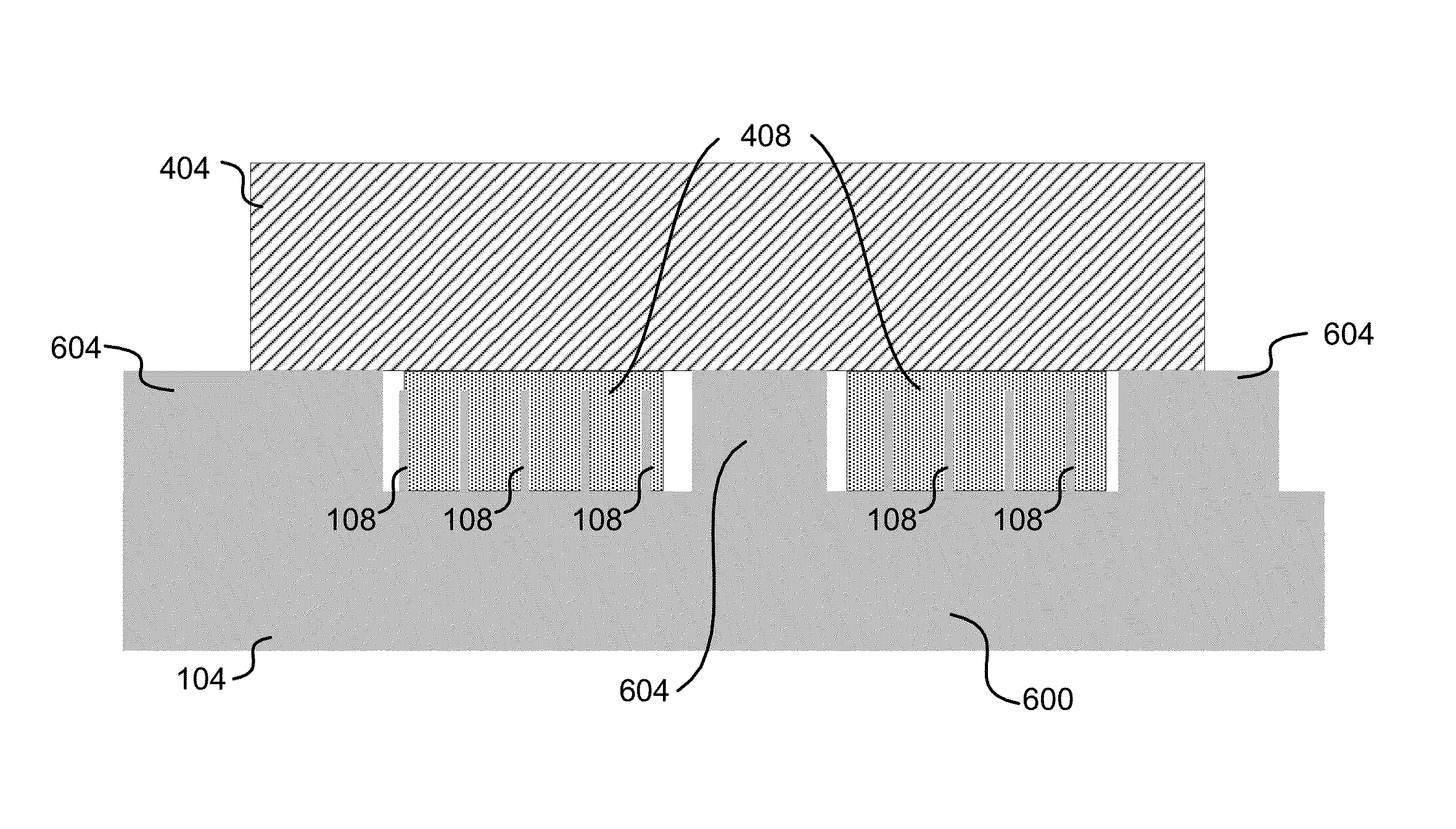
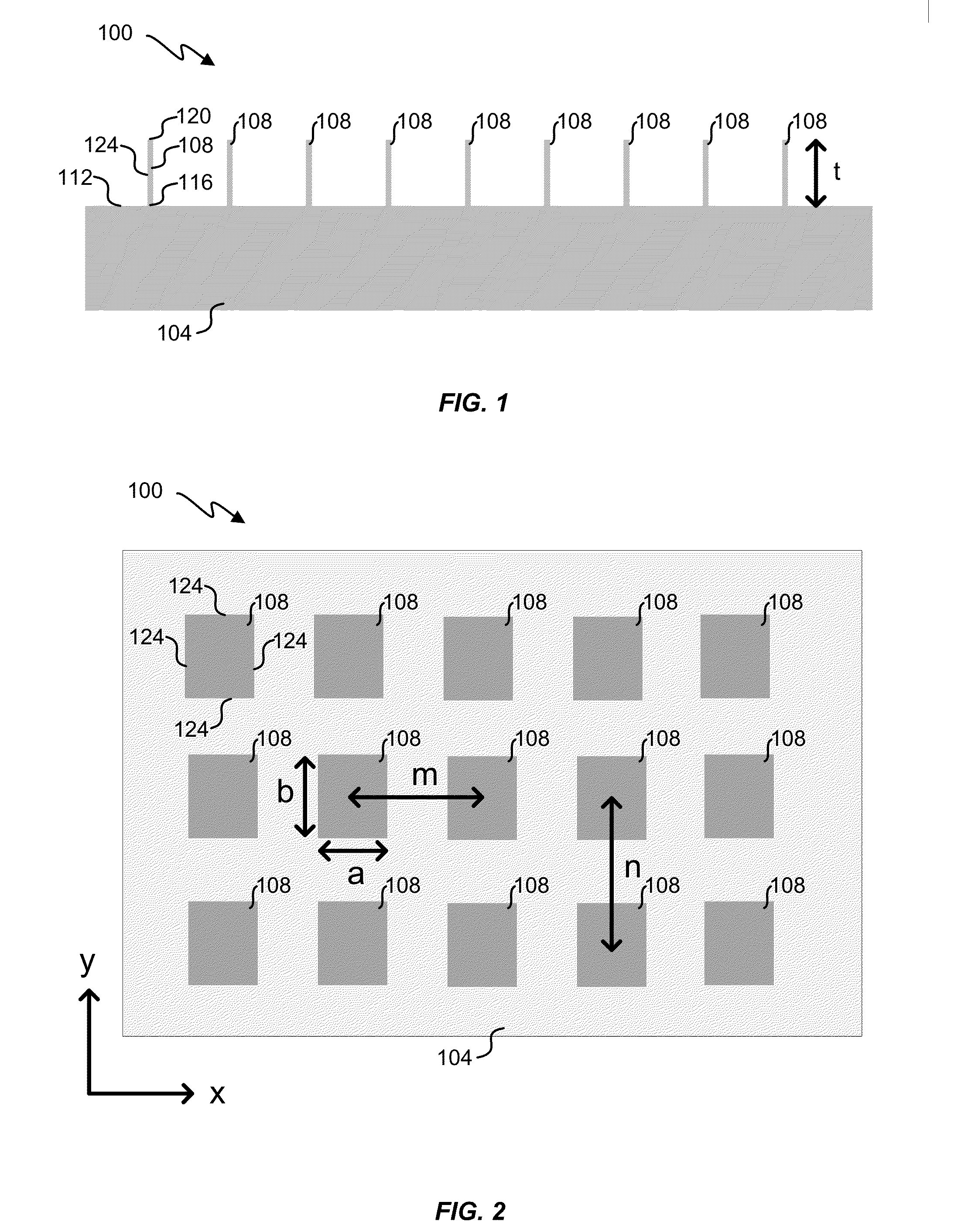
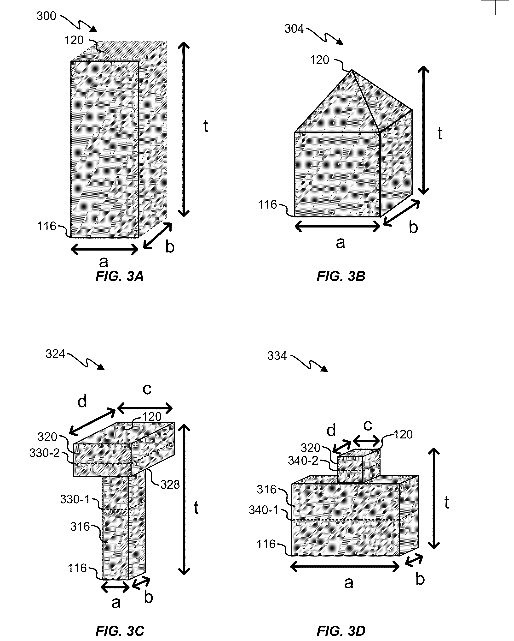
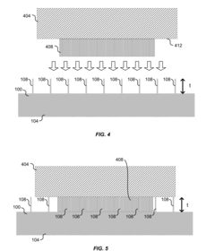
Existing Silicon Micropillar Fabrication Techniques
01 Fabrication methods for silicon micropillars
Various techniques are employed to create silicon micropillars, including etching processes, lithography, and deposition methods. These fabrication methods allow for precise control over the size, shape, and spacing of the micropillars, which is crucial for their performance in different applications.- Fabrication methods for silicon micropillars: Various techniques are employed to create silicon micropillars, including etching processes, lithography, and deposition methods. These fabrication methods allow for precise control over the size, shape, and arrangement of the micropillars, which is crucial for their performance in different applications.
- Applications in solar cells and photovoltaics: Silicon micropillars are utilized in solar cell and photovoltaic technologies to enhance light absorption and improve overall efficiency. The unique structure of micropillars allows for better light trapping and increased surface area, leading to improved energy conversion rates.
- Use in microfluidic and lab-on-a-chip devices: Silicon micropillars play a significant role in microfluidic systems and lab-on-a-chip devices. They can be used for fluid manipulation, particle separation, and as structural elements in miniaturized analytical systems, enabling more efficient and precise biomedical and chemical analyses.
- Integration with MEMS and sensor technologies: Silicon micropillars are integrated into Micro-Electro-Mechanical Systems (MEMS) and various sensor technologies. Their unique properties allow for the development of highly sensitive and miniaturized sensors for applications in environmental monitoring, biomedical devices, and industrial process control.
- Surface modification and functionalization: The surface of silicon micropillars can be modified and functionalized to enhance their properties or add new functionalities. This includes coating with various materials, chemical treatments, or the addition of specific molecules to tailor the micropillars for particular applications such as improved wettability, biocompatibility, or sensing capabilities.
02 Applications in solar cells and photovoltaics
Silicon micropillars are utilized in solar cell and photovoltaic technologies to enhance light absorption and improve overall efficiency. The unique structure of micropillars allows for better light trapping and increased surface area, leading to improved energy conversion rates.Expand Specific Solutions03 Use in microfluidic and lab-on-a-chip devices
Silicon micropillars play a significant role in microfluidic systems and lab-on-a-chip devices. They can be used for fluid manipulation, particle separation, and as structural elements in miniaturized analytical systems, enabling more efficient and precise microfluidic operations.Expand Specific Solutions04 Integration with MEMS and sensor technologies
Silicon micropillars are integrated into Micro-Electro-Mechanical Systems (MEMS) and various sensor technologies. Their unique properties allow for enhanced sensitivity and functionality in applications such as pressure sensors, accelerometers, and chemical sensors.Expand Specific Solutions05 Surface modification and functionalization
The surface of silicon micropillars can be modified and functionalized to tailor their properties for specific applications. This includes coating with various materials, chemical treatments, and the addition of functional groups to enhance their performance in areas such as biosensing, catalysis, and wettability control.Expand Specific Solutions
Key Players in Microelectronic Device Industry
The analysis of Silicon Micropillars in Microelectronic Devices is currently in a growth phase, with increasing market size and technological advancements. The competitive landscape is characterized by a mix of established semiconductor companies and research institutions. Key players like Micron Technology, IBM, and Samsung Electronics are driving innovation, while academic institutions such as Caltech and Georgia Tech contribute to fundamental research. The technology's maturity is progressing, with companies like GLOBALFOUNDRIES and Infineon Technologies actively developing applications. However, the field remains dynamic, with emerging players like Nexeon and Skorpios Technologies introducing novel approaches, indicating ongoing opportunities for technological breakthroughs and market expansion.
International Business Machines Corp.
Technical Solution: IBM has developed advanced silicon micropillar technology for microelectronic devices, focusing on enhancing performance and efficiency. Their approach involves creating high-aspect-ratio silicon pillars with diameters ranging from 50 to 200 nanometers and heights up to several micrometers [1]. These structures are fabricated using a combination of deep reactive ion etching (DRIE) and advanced lithography techniques. IBM's silicon micropillars are designed to improve heat dissipation in high-performance computing chips, potentially increasing processing speeds by up to 15% [3]. Additionally, they have explored the use of these micropillars in 3D integrated circuits, allowing for higher device density and improved interconnect performance [5].
Strengths: Superior heat dissipation, increased processing speeds, and higher device density. Weaknesses: Complex fabrication process, potential for structural instability in extreme conditions.
Samsung Electronics Co., Ltd.
Technical Solution: Samsung has developed silicon micropillar technology for a wide range of microelectronic devices, including memory, logic, and image sensors. Their approach involves creating silicon pillars with diameters ranging from 10 to 100 nanometers and heights up to several hundred nanometers [2]. These structures are fabricated using a combination of advanced lithography, selective epitaxial growth, and atomic layer deposition techniques. Samsung's silicon micropillars are designed to improve the performance of DRAM and NAND flash memory, potentially increasing storage density by up to 8 times compared to conventional planar designs [4]. In logic devices, these micropillars have been used to create gate-all-around (GAA) transistors, potentially improving performance by up to 35% while reducing power consumption by up to 50% [6]. Samsung has also explored the use of silicon micropillars in image sensors, potentially improving light sensitivity by up to 40% [7].
Strengths: Versatile technology applicable to multiple device types, significant improvements in performance and density. Weaknesses: Complex integration challenges, potential reliability issues at extreme scaling.
Core Innovations in Micropillar Design
Micro-pillar assisted semiconductor bonding
PatentActiveUS20150364441A1
Innovation
- The use of micro pillars on the silicon substrate to penetrate and break indium oxide, reducing the initial surface contact area and heat transfer, allowing for easier melting of indium and improved bonding by modulating heat and pressure transfer.
Microelectronic devices including semiconductive pillar structures, and related electronic systems
PatentActiveUS11812603B2
Innovation
- The design incorporates semiconductive pillar structures with angled end portions relative to the central portion, increasing the distance between storage node contact regions and bit line contact regions, and using advanced patterning techniques like pitch quadrupling and spacer-assisted double patterning to form these structures, reducing the likelihood of shorting and enhancing mechanical stability.
Environmental Impact of Micropillar Production
The production of silicon micropillars for microelectronic devices has significant environmental implications that warrant careful consideration. The manufacturing process involves several stages, each with its own environmental impact.
The initial stage of silicon wafer production requires substantial energy consumption and generates greenhouse gas emissions. The high-purity silicon needed for micropillars is obtained through energy-intensive processes, including the reduction of silica in electric arc furnaces. This process contributes to carbon dioxide emissions and requires large amounts of electricity, often sourced from fossil fuels.
Chemical etching, a crucial step in micropillar fabrication, utilizes various hazardous chemicals such as hydrofluoric acid and sulfuric acid. These chemicals pose risks to both human health and the environment if not properly managed. Proper disposal and treatment of these chemical waste streams are essential to prevent soil and water contamination.
Water usage is another critical environmental concern in micropillar production. The manufacturing process requires ultra-pure water for cleaning and rinsing, leading to high water consumption. This can strain local water resources, particularly in water-scarce regions where many semiconductor facilities are located.
The use of rare earth elements and precious metals in the production process also raises sustainability concerns. Mining and refining these materials often involve environmentally destructive practices and can lead to habitat destruction and biodiversity loss in mining regions.
Waste management is a significant challenge in micropillar production. The process generates various types of waste, including silicon wafer scraps, used chemicals, and contaminated water. Proper recycling and disposal methods are crucial to minimize environmental impact and recover valuable materials.
Energy efficiency in the production process is an ongoing concern. The need for cleanroom environments and precise temperature control contributes to high energy consumption. Improving energy efficiency in these processes is essential for reducing the overall environmental footprint of micropillar production.
As the demand for microelectronic devices continues to grow, the cumulative environmental impact of micropillar production becomes increasingly significant. This necessitates ongoing research and development into more sustainable production methods, including the use of renewable energy sources, closed-loop water systems, and less hazardous chemical alternatives.
Scaling Limitations and Solutions
The scaling of silicon micropillars in microelectronic devices faces significant limitations as dimensions approach the nanoscale. One primary challenge is the increased surface-to-volume ratio, which leads to enhanced surface effects and altered material properties. This phenomenon can result in unexpected electrical and mechanical behaviors, potentially compromising device performance and reliability.
Another critical limitation is the quantum confinement effect, which becomes prominent as the pillar dimensions approach the de Broglie wavelength of electrons. This effect can dramatically change the electronic band structure and carrier transport properties, necessitating new design paradigms and modeling approaches for device optimization.
Fabrication challenges also emerge at smaller scales. Conventional lithography techniques struggle to achieve the required precision and uniformity for sub-10 nm features. Additionally, etching processes become increasingly difficult to control, leading to non-uniform pillar shapes and sizes, which can introduce variability in device characteristics.
To address these scaling limitations, several innovative solutions have been proposed and implemented. Advanced lithography techniques, such as extreme ultraviolet (EUV) lithography and directed self-assembly, offer improved resolution and pattern fidelity for creating smaller micropillars. These methods enable the fabrication of more uniform and densely packed structures, pushing the boundaries of device miniaturization.
Novel materials and heterostructures are being explored to mitigate the adverse effects of scaling. For instance, incorporating strain engineering or using core-shell structures can help maintain desirable electrical properties even at reduced dimensions. Similarly, the integration of high-k dielectrics and metal gates has proven effective in managing leakage currents and improving electrostatic control in scaled devices.
Three-dimensional architectures, such as vertical nanowires and fin-based structures, offer an alternative approach to overcome planar scaling limitations. These designs provide better electrostatic control and increased current drive per unit area, enabling continued performance improvements without relying solely on lateral scaling.
Advanced modeling and simulation tools have become indispensable for predicting and optimizing the behavior of scaled silicon micropillars. Quantum mechanical simulations and multi-scale modeling approaches allow designers to account for complex physical phenomena and guide the development of next-generation devices.
Unlock deeper insights with Patsnap Eureka Quick Research — get a full tech report to explore trends and direct your research. Try now!
Generate Your Research Report Instantly with AI Agent
Supercharge your innovation with Patsnap Eureka AI Agent Platform!