Silicon Micropillars for Advanced Electromagnetic Interference Shielding
JUL 9, 20258 MIN READ
Generate Your Research Report Instantly with AI Agent
Patsnap Eureka helps you evaluate technical feasibility & market potential.
EMI Shielding Evolution
Electromagnetic Interference (EMI) shielding has evolved significantly over the past decades, driven by the increasing complexity and miniaturization of electronic devices. The journey of EMI shielding began in the mid-20th century with the widespread adoption of electronic equipment in various industries. Initially, simple metal enclosures were used to contain electromagnetic emissions and protect sensitive components from external interference.
As electronic devices became more compact and powerful, traditional shielding methods proved inadequate. The 1980s and 1990s saw the introduction of conductive coatings and gaskets, which offered improved flexibility and adaptability to various form factors. These innovations allowed for better integration of shielding solutions into complex electronic designs.
The turn of the millennium marked a significant shift towards advanced materials in EMI shielding. Conductive polymers and composite materials emerged as promising alternatives to traditional metal-based shields. These materials offered advantages such as lightweight construction, corrosion resistance, and the ability to be molded into intricate shapes, making them ideal for modern electronic devices.
In recent years, nanotechnology has revolutionized EMI shielding techniques. The development of nanomaterials like carbon nanotubes, graphene, and metal nanoparticles has led to ultra-thin, highly effective shielding solutions. These materials exhibit exceptional electromagnetic absorption and reflection properties, allowing for superior shielding performance without adding significant bulk or weight to devices.
The latest frontier in EMI shielding evolution is the exploration of engineered structures at the micro and nanoscale. Silicon micropillars represent a cutting-edge approach in this domain. By precisely controlling the geometry and arrangement of these microscopic structures, researchers aim to create highly effective EMI shields that can be seamlessly integrated into semiconductor devices.
The evolution of EMI shielding technologies has been closely tied to advancements in material science, fabrication techniques, and the ever-increasing demands of the electronics industry. As devices continue to shrink and operate at higher frequencies, the need for innovative shielding solutions becomes more critical. The development of silicon micropillars for EMI shielding represents a convergence of semiconductor technology and electromagnetic protection, potentially opening new avenues for integrated shielding solutions in next-generation electronic devices.
Market Demand Analysis
The market demand for advanced electromagnetic interference (EMI) shielding solutions, particularly those utilizing silicon micropillars, has been steadily increasing in recent years. This growth is primarily driven by the rapid expansion of electronic devices and systems across various industries, including telecommunications, automotive, aerospace, and consumer electronics.
The proliferation of 5G technology and the Internet of Things (IoT) has significantly contributed to the rising demand for effective EMI shielding. As these technologies require higher frequency operations and more compact device designs, traditional shielding methods are becoming less effective. Silicon micropillars offer a promising solution to this challenge, providing superior shielding performance in a compact form factor.
In the automotive sector, the transition towards electric and autonomous vehicles has created a substantial market for advanced EMI shielding. These vehicles incorporate numerous electronic systems that must operate in close proximity without interference, making effective shielding crucial for safety and performance.
The aerospace and defense industries also represent significant market opportunities for silicon micropillar-based EMI shielding. The increasing use of electronic systems in aircraft and military equipment demands robust shielding solutions that can withstand harsh environmental conditions while maintaining optimal performance.
Consumer electronics, including smartphones, tablets, and wearable devices, continue to drive demand for innovative EMI shielding solutions. As these devices become more powerful and compact, the need for effective shielding in limited spaces becomes more critical, making silicon micropillars an attractive option.
The healthcare sector is emerging as a potential growth area for advanced EMI shielding. Medical devices and equipment often operate in electromagnetically sensitive environments, requiring reliable shielding to ensure accurate diagnostics and treatment.
Market analysts predict that the global EMI shielding market will continue to grow at a compound annual growth rate (CAGR) of over 5% in the coming years. The silicon micropillar segment is expected to outpace this growth rate due to its superior performance characteristics and adaptability to various applications.
However, challenges such as high initial costs and the need for specialized manufacturing processes may initially limit widespread adoption. As production techniques improve and economies of scale are achieved, these barriers are expected to diminish, further driving market growth for silicon micropillar-based EMI shielding solutions.
Silicon Micropillar Tech
Silicon micropillars represent a cutting-edge technology in the field of electromagnetic interference (EMI) shielding. These structures, typically fabricated from silicon, are designed to effectively attenuate electromagnetic waves across a wide frequency spectrum. The development of silicon micropillars for EMI shielding has been driven by the increasing demand for more efficient and compact shielding solutions in various electronic applications.
The fundamental principle behind silicon micropillar technology lies in its ability to create a high-impedance surface that can reflect and absorb electromagnetic waves. The micropillars, arranged in specific patterns and geometries, interact with incident electromagnetic radiation, causing multiple reflections and scattering events. This interaction leads to the dissipation of electromagnetic energy, effectively reducing the transmission of EMI through the material.
One of the key advantages of silicon micropillars is their scalability and compatibility with existing semiconductor manufacturing processes. This allows for seamless integration into various electronic devices and systems, making them particularly attractive for applications in miniaturized and high-frequency electronics. The ability to precisely control the dimensions and spacing of the micropillars enables fine-tuning of their EMI shielding properties for specific frequency ranges.
Recent advancements in silicon micropillar technology have focused on enhancing their performance through various strategies. These include optimizing the pillar geometry, incorporating conductive coatings, and developing hybrid structures that combine micropillars with other materials. For instance, researchers have explored the use of metal-coated silicon micropillars to improve conductivity and overall shielding effectiveness.
The fabrication of silicon micropillars typically involves advanced microfabrication techniques such as photolithography, deep reactive ion etching (DRIE), and chemical vapor deposition (CVD). These processes allow for the creation of high-aspect-ratio structures with precise control over their dimensions and spacing. The ongoing research in this field aims to develop more cost-effective and scalable manufacturing methods to facilitate widespread adoption of this technology.
As the demand for EMI shielding continues to grow in sectors such as 5G communications, automotive electronics, and aerospace, silicon micropillar technology is poised to play a crucial role. Its potential to provide superior shielding performance while maintaining a low profile and lightweight characteristics makes it an attractive solution for next-generation electronic devices and systems.
Current EMI Solutions
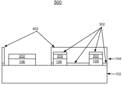
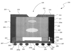
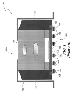
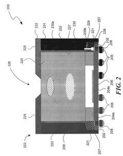
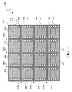
01 Silicon micropillar structures for EMI shielding
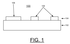
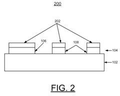
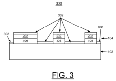
Silicon micropillars can be fabricated on substrates to create effective electromagnetic interference (EMI) shielding structures. These micropillars can be designed with specific dimensions and arrangements to attenuate electromagnetic waves across a wide frequency range. The high aspect ratio and conductivity of silicon make it an ideal material for creating these shielding structures.- Silicon micropillar structures for EMI shielding: Silicon micropillars can be fabricated on substrates to create effective electromagnetic interference (EMI) shielding structures. These micropillars can be designed with specific dimensions and arrangements to attenuate electromagnetic waves across a wide frequency range. The high aspect ratio and conductivity of silicon make it an ideal material for creating these shielding structures.
- Conductive coatings on silicon micropillars: Applying conductive coatings, such as metal layers or conductive polymers, on silicon micropillars can enhance their EMI shielding effectiveness. These coatings increase the overall conductivity of the structure and improve its ability to reflect and absorb electromagnetic waves. The combination of the micropillar geometry and conductive coating creates a highly effective EMI shielding solution.
- Integration of silicon micropillars in electronic packaging: Silicon micropillars can be integrated into electronic packaging solutions to provide localized EMI shielding. This approach allows for targeted protection of sensitive components within electronic devices. The micropillars can be fabricated directly on package substrates or incorporated as separate elements, offering flexibility in design and implementation for various electronic applications.
- Hybrid EMI shielding solutions with silicon micropillars: Combining silicon micropillars with other EMI shielding materials or techniques can create hybrid solutions with enhanced performance. This may include incorporating micropillars with traditional metal shields, conductive fabrics, or absorptive materials. The synergistic effect of these combinations can provide superior EMI shielding across a broader spectrum of frequencies and applications.
- Fabrication techniques for silicon micropillar EMI shields: Various fabrication techniques can be employed to create silicon micropillar structures for EMI shielding. These may include etching processes, lithography, and growth methods. Advanced fabrication techniques allow for precise control over micropillar dimensions, spacing, and patterns, enabling optimization of the shielding performance for specific frequency ranges and applications.
02 Conductive coatings on silicon micropillars
Applying conductive coatings, such as metal layers or conductive polymers, on silicon micropillars can enhance their EMI shielding effectiveness. These coatings increase the overall conductivity of the structure and improve its ability to reflect and absorb electromagnetic waves. The combination of the micropillar geometry and conductive coating creates a highly effective shielding solution.Expand Specific Solutions03 Integration of silicon micropillars in electronic packaging
Silicon micropillars can be integrated into electronic packaging solutions to provide localized EMI shielding. This approach allows for targeted protection of sensitive components within a device. The micropillars can be fabricated directly on package substrates or incorporated as separate elements, offering flexibility in design and implementation for various electronic applications.Expand Specific Solutions04 Hybrid shielding solutions combining silicon micropillars with other materials
Combining silicon micropillars with other shielding materials, such as conductive foams, meshes, or nanocomposites, can create hybrid EMI shielding solutions. These hybrid structures leverage the unique properties of each material to achieve superior shielding performance across a broader frequency spectrum. The synergistic effect of multiple shielding mechanisms enhances overall effectiveness.Expand Specific Solutions05 Tunable EMI shielding using silicon micropillar arrays
Arrays of silicon micropillars can be designed with varying heights, spacings, and patterns to create tunable EMI shielding solutions. By adjusting these parameters, the shielding effectiveness can be optimized for specific frequency ranges or applications. This tunability allows for customized shielding solutions that can adapt to different electromagnetic environments or device requirements.Expand Specific Solutions
Key Industry Players
The research on silicon micropillars for advanced electromagnetic interference shielding is in an emerging phase, with growing market potential due to increasing demand for EMI shielding in electronics and telecommunications. The technology is still evolving, with varying levels of maturity among key players. Companies like Taiwan Semiconductor Manufacturing Co., Hon Hai Precision Industry, and Infineon Technologies AG are at the forefront, leveraging their semiconductor expertise. Other players such as Laird Technologies and Nitto Denko Corp. are also making significant contributions. The competitive landscape is diverse, with both established semiconductor giants and specialized materials companies vying for market share in this promising field.
Taiwan Semiconductor Manufacturing Co., Ltd.
Technical Solution: TSMC has invested in silicon micropillar technology for EMI shielding in advanced semiconductor packaging. Their approach focuses on integrating EMI shielding directly into the chip package using through-silicon vias (TSVs) and silicon micropillars. TSMC's process involves creating high-density arrays of silicon micropillars on the chip surface, which are then metallized to form a conductive shield. This technique allows for EMI shielding at the chip level, reducing interference between different components in complex system-in-package (SiP) designs[3]. TSMC has also developed methods to combine silicon micropillars with on-chip antennas for 5G and mmWave applications, enabling improved signal integrity while maintaining effective EMI shielding[4]. The company's research includes optimizing the micropillar geometry and metallization process to achieve the best balance between shielding effectiveness and minimal impact on chip performance.
Strengths: Integrated chip-level EMI shielding, compatibility with advanced packaging technologies. Weaknesses: Limited to semiconductor applications, potentially higher cost per chip compared to external shielding solutions.
3M Innovative Properties Co.
Technical Solution: 3M has developed advanced silicon micropillar structures for electromagnetic interference (EMI) shielding. Their approach involves creating high-aspect-ratio silicon micropillars with nanoscale features, which are then coated with conductive materials. This design enhances the surface area for EMI absorption while maintaining a thin overall profile. The micropillars are fabricated using deep reactive ion etching (DRIE) techniques, allowing for precise control over pillar dimensions and spacing[1]. 3M's silicon micropillars are integrated into flexible polymer matrices, creating adaptable EMI shielding materials that can conform to complex surfaces. The company has also explored incorporating graphene and other 2D materials into the micropillar structures to further improve shielding effectiveness across a wide frequency range[2].
Strengths: High shielding effectiveness, flexibility, and adaptability to various surfaces. Weaknesses: Potentially higher production costs compared to traditional shielding materials, and challenges in scaling up production for large-area applications.
Micropillar Innovations
Structures for implementing EMI shielding for rigid cards and flexible circuits
PatentInactiveUS20080236883A1
Innovation
- A thin electrically conductive copper coating is applied using vacuum sputtering deposition, embedded within a solder mask, to form an EMI shielding boundary without the need for conventional external copper layers, allowing for mechanical cleaning in unprotected areas and maintaining electromagnetic compatibility (EMC) without added complexity or cost.
Integrated conductive shield for microelectronic device assemblies and associated methods
PatentInactiveUS20090243051A1
Innovation
- A conductive shield structure is integrated into the imager assembly, comprising a layer of conductive material in contact with the objective lens and a dielectric sidewall, with a shield interconnect providing a conductive path to ground, reducing the overall footprint while effectively suppressing electromagnetic interference.
Material Characterization
Material characterization plays a crucial role in understanding and optimizing the performance of silicon micropillars for advanced electromagnetic interference (EMI) shielding. The unique properties of silicon at the microscale contribute significantly to its effectiveness in EMI shielding applications.
The characterization of silicon micropillars begins with an analysis of their physical structure. Scanning electron microscopy (SEM) and atomic force microscopy (AFM) are commonly employed to examine the surface morphology, pillar dimensions, and spatial distribution. These techniques provide valuable insights into the uniformity and consistency of the micropillar arrays, which directly impact their EMI shielding capabilities.
X-ray diffraction (XRD) analysis is utilized to investigate the crystalline structure of the silicon micropillars. This method reveals information about the crystal orientation, lattice parameters, and any potential defects or impurities present in the material. Understanding the crystalline nature of the micropillars is essential for predicting and optimizing their electromagnetic properties.
Electrical characterization of silicon micropillars is conducted through various techniques, including four-point probe measurements and Hall effect measurements. These methods provide data on the electrical resistivity, carrier concentration, and mobility of the material. Such information is crucial for determining the micropillars' ability to interact with electromagnetic waves and dissipate energy effectively.
The optical properties of silicon micropillars are assessed using spectroscopic techniques such as UV-Vis-NIR spectroscopy and ellipsometry. These measurements offer insights into the material's refractive index, absorption coefficient, and bandgap, which influence its interaction with electromagnetic radiation across different wavelengths.
Thermal characterization is another important aspect, as the performance of EMI shielding materials can be temperature-dependent. Techniques like differential scanning calorimetry (DSC) and thermogravimetric analysis (TGA) are employed to study the thermal stability and phase transitions of silicon micropillars under various conditions.
Surface chemical analysis techniques, including X-ray photoelectron spectroscopy (XPS) and Fourier-transform infrared spectroscopy (FTIR), are used to examine the surface composition and chemical bonding of the micropillars. This information is valuable for understanding potential surface modifications or treatments that may enhance EMI shielding performance.
Mechanical properties of silicon micropillars are evaluated using nanoindentation and atomic force microscopy-based techniques. These methods provide data on the hardness, elastic modulus, and mechanical stability of the micropillars, which are essential for ensuring the durability and reliability of the EMI shielding material in practical applications.
Fabrication Techniques
The fabrication of silicon micropillars for advanced electromagnetic interference (EMI) shielding involves several sophisticated techniques. One of the primary methods is photolithography, which allows for precise patterning of the micropillar structures. This process begins with the deposition of a photoresist layer on a silicon wafer, followed by exposure to UV light through a mask with the desired micropillar pattern. The exposed areas are then developed, leaving a template for the micropillars.
Etching techniques play a crucial role in creating the high-aspect-ratio structures characteristic of silicon micropillars. Deep reactive ion etching (DRIE) is particularly effective, utilizing alternating cycles of etching and passivation to achieve vertical sidewalls and deep trenches. The Bosch process, a specific DRIE technique, is widely employed for its ability to create highly anisotropic features with excellent control over pillar dimensions and spacing.
Another approach to fabricating silicon micropillars is metal-assisted chemical etching (MacEtch). This method involves depositing a thin metal layer, typically gold or silver, on the silicon surface. The metal acts as a catalyst, accelerating the etching of silicon in the presence of an oxidizing agent and hydrofluoric acid. MacEtch offers the advantage of producing high-aspect-ratio structures without the need for expensive equipment.
For more complex micropillar designs, such as those with varying diameters or tapered profiles, a combination of techniques may be employed. Focused ion beam (FIB) milling can be used for fine-tuning the micropillar geometry or creating specialized features. Additionally, atomic layer deposition (ALD) can be utilized to coat the micropillars with thin, conformal layers of materials that enhance their EMI shielding properties.
The choice of fabrication technique depends on factors such as the desired micropillar dimensions, aspect ratio, and surface properties. Each method has its strengths and limitations in terms of scalability, cost-effectiveness, and achievable feature sizes. As research in this field progresses, new hybrid approaches and refinements to existing techniques are continually being developed to optimize the fabrication process and enhance the EMI shielding performance of silicon micropillars.
Unlock deeper insights with Patsnap Eureka Quick Research — get a full tech report to explore trends and direct your research. Try now!
Generate Your Research Report Instantly with AI Agent
Supercharge your innovation with Patsnap Eureka AI Agent Platform!