What Silicon Micropillars Offer to 3D Printing Technologies
JUL 9, 20259 MIN READ
Generate Your Research Report Instantly with AI Agent
Patsnap Eureka helps you evaluate technical feasibility & market potential.
Silicon Micropillars in 3D Printing: Background and Objectives
Silicon micropillars have emerged as a groundbreaking technology in the field of 3D printing, offering unprecedented possibilities for enhancing the precision, functionality, and versatility of additive manufacturing processes. The development of silicon micropillars represents a convergence of nanotechnology, materials science, and advanced manufacturing techniques, aiming to address longstanding challenges in 3D printing technologies.
The evolution of 3D printing has been marked by continuous efforts to improve resolution, material properties, and printing speed. Traditional 3D printing methods, while revolutionary, have faced limitations in achieving nanoscale precision and incorporating advanced functionalities into printed objects. Silicon micropillars have emerged as a potential solution to these challenges, leveraging the unique properties of silicon at the microscale.
The primary objective of integrating silicon micropillars into 3D printing is to enable the creation of structures with enhanced mechanical, electrical, and optical properties. By incorporating these microscale features, researchers and engineers aim to expand the applications of 3D printing in fields such as microelectronics, biomedical devices, and advanced sensors.
Silicon micropillars offer several key advantages in 3D printing. Their high aspect ratio and controllable dimensions allow for the creation of complex, three-dimensional structures with unprecedented precision. The semiconductor properties of silicon also open up possibilities for integrating electronic functionalities directly into printed objects, paving the way for smart, multifunctional devices.
The development of silicon micropillar technology for 3D printing is driven by the growing demand for miniaturization and increased functionality in various industries. From more efficient solar cells to advanced medical implants, the potential applications of this technology are vast and diverse.
As the field progresses, researchers are focusing on overcoming challenges related to scalability, integration with existing 3D printing platforms, and optimizing the properties of silicon micropillars for specific applications. The ultimate goal is to establish silicon micropillars as a versatile tool in the 3D printing toolkit, enabling the creation of next-generation devices and materials with unprecedented capabilities.
This technological advancement represents a significant step towards bridging the gap between nanoscale fabrication and macroscale manufacturing, potentially revolutionizing how we design and produce complex, functional objects across multiple industries.
Market Analysis for Advanced 3D Printing Materials
The market for advanced 3D printing materials, particularly those incorporating silicon micropillars, is experiencing significant growth and transformation. This emerging technology offers unique advantages in terms of precision, durability, and functionality, driving increased demand across various industries. The global 3D printing materials market is projected to expand rapidly, with silicon-based materials playing a crucial role in this growth.
Silicon micropillars represent a breakthrough in 3D printing materials, offering enhanced structural integrity and improved surface properties. These materials are particularly valuable in industries requiring high-precision components, such as aerospace, automotive, and medical devices. The ability to create intricate, micro-scale structures with silicon micropillars opens up new possibilities for product design and manufacturing processes.
The adoption of silicon micropillar technology in 3D printing is driven by several key factors. Firstly, the increasing demand for lightweight yet strong materials in aerospace and automotive industries is fueling research and development in this area. Secondly, the growing need for biocompatible materials in medical applications is pushing the boundaries of what's possible with silicon-based 3D printing materials.
Market trends indicate a shift towards more specialized and high-performance materials in the 3D printing industry. Silicon micropillars are at the forefront of this trend, offering superior mechanical properties and the potential for multifunctional materials. This technology is particularly appealing in the production of sensors, microfluidic devices, and advanced electronic components.
The market for silicon micropillar-based 3D printing materials is still in its early stages but shows promising growth potential. Early adopters in research institutions and high-tech industries are driving initial demand, with wider commercial applications expected to follow as the technology matures. The unique properties of silicon micropillars, such as their ability to create highly precise structures at the microscale, position them as a premium segment within the broader 3D printing materials market.
Challenges in the market include the relatively high cost of production and the need for specialized equipment to fully utilize the capabilities of silicon micropillar materials. However, ongoing research and development efforts are focused on addressing these barriers, potentially leading to more cost-effective solutions in the near future.
As the technology advances, the market for silicon micropillar-based 3D printing materials is expected to expand into new application areas. Potential growth sectors include energy storage devices, advanced optics, and next-generation semiconductor manufacturing. The versatility of silicon as a material, combined with the precision offered by micropillar structures, presents a wide range of possibilities for innovation across multiple industries.
Current Challenges in 3D Printing with Silicon
3D printing with silicon faces several significant challenges that hinder its widespread adoption and application. One of the primary obstacles is the high melting point of silicon, which exceeds 1400°C. This extreme temperature requirement makes it difficult to process silicon using conventional 3D printing techniques, as most printers are not designed to operate at such high temperatures.
Another major challenge is the rapid oxidation of silicon when exposed to air at high temperatures. This oxidation process can lead to the formation of silicon dioxide layers, which can compromise the structural integrity and electrical properties of the printed silicon components. Preventing oxidation during the printing process requires sophisticated environmental control systems, adding complexity and cost to the manufacturing setup.
The thermal expansion of silicon during heating and cooling cycles poses additional difficulties. Silicon's coefficient of thermal expansion can cause warping, cracking, or delamination of printed structures, especially in complex geometries or when printing large objects. This thermal behavior necessitates careful control of heating and cooling rates, as well as the development of specialized support structures and printing strategies.
Furthermore, achieving high purity in 3D-printed silicon structures is challenging. Impurities introduced during the printing process can significantly affect the electrical and mechanical properties of the final product. This is particularly critical for applications in electronics and photovoltaics, where material purity is paramount for optimal performance.
The resolution and surface finish of 3D-printed silicon structures also present ongoing challenges. Current technologies often struggle to produce silicon components with the fine features and smooth surfaces required for many high-tech applications. This limitation restricts the use of 3D-printed silicon in areas such as microelectronics and optical devices.
Lastly, the high cost and limited availability of suitable silicon materials for 3D printing pose economic challenges. Most existing 3D printing technologies are optimized for polymers or metals, and adapting them for silicon processing often requires significant modifications and investments. The development of cost-effective, high-quality silicon feedstock materials specifically designed for 3D printing remains an active area of research and development.
Addressing these challenges requires interdisciplinary efforts combining materials science, thermal engineering, and advanced manufacturing techniques. Overcoming these hurdles will be crucial for unlocking the full potential of silicon in 3D printing technologies and enabling new applications in fields such as electronics, energy, and biomedical engineering.
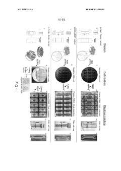
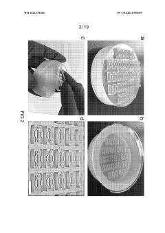
Existing Silicon Micropillar Integration Methods
01 Fabrication methods for silicon micropillars
Various techniques are employed to create silicon micropillars, including etching processes, lithography, and deposition methods. These fabrication methods allow for precise control over the size, shape, and arrangement of the micropillars, which is crucial for their performance in different applications.- Fabrication methods for silicon micropillars: Various techniques are employed to create silicon micropillars, including etching processes, lithography, and deposition methods. These fabrication methods allow for precise control over the size, shape, and arrangement of the micropillars, which is crucial for their performance in different applications.
- Applications in solar cells and photovoltaics: Silicon micropillars are utilized in solar cell and photovoltaic technologies to enhance light absorption and improve overall efficiency. The unique structure of micropillars allows for better light trapping and increased surface area, leading to improved energy conversion rates.
- Use in microfluidic and lab-on-a-chip devices: Silicon micropillars play a significant role in microfluidic systems and lab-on-a-chip devices. They can be used for fluid manipulation, particle separation, and as structural elements in miniaturized analytical systems, enabling more efficient and precise control of small-scale fluid dynamics.
- Integration with sensors and MEMS devices: Silicon micropillars are integrated into various sensors and MEMS (Micro-Electro-Mechanical Systems) devices. Their unique properties allow for enhanced sensitivity in chemical and biological sensors, as well as improved performance in mechanical sensing applications.
- Surface modification and functionalization: The surface of silicon micropillars can be modified and functionalized to tailor their properties for specific applications. This includes coating with various materials, chemical treatments, and the addition of functional groups to enhance their performance in areas such as catalysis, sensing, and biomedical applications.
02 Applications in solar cells and photovoltaics
Silicon micropillars are utilized in solar cell and photovoltaic technologies to enhance light absorption and improve overall efficiency. The unique structure of micropillars allows for better light trapping and increased surface area, leading to improved energy conversion rates.Expand Specific Solutions03 Use in microfluidic and lab-on-a-chip devices
Silicon micropillars play a significant role in microfluidic systems and lab-on-a-chip devices. They can be used for fluid manipulation, particle separation, and as support structures for various biochemical processes, enhancing the functionality and efficiency of these miniaturized systems.Expand Specific Solutions04 Integration with sensors and MEMS devices
Silicon micropillars are integrated into various sensors and MEMS (Micro-Electro-Mechanical Systems) devices. Their unique properties allow for enhanced sensitivity, improved mechanical stability, and increased surface area for sensing applications, leading to more efficient and compact sensor designs.Expand Specific Solutions05 Surface modification and functionalization
The surface of silicon micropillars can be modified and functionalized to tailor their properties for specific applications. This includes coating with various materials, chemical treatments, and the addition of functional groups to enhance their performance in areas such as catalysis, biomedical applications, and advanced materials.Expand Specific Solutions
Key Players in Silicon Micropillar 3D Printing
The development of silicon micropillars in 3D printing technologies represents an emerging field at the intersection of materials science and additive manufacturing. This sector is in its early growth stage, with significant potential for expansion as the technology matures. The market size is currently modest but expected to grow rapidly as applications in microelectronics, sensors, and biomedical devices become more prevalent. In terms of technological maturity, silicon micropillar 3D printing is still evolving, with ongoing research and development efforts led by institutions like MIT, Johns Hopkins University, and Huazhong University of Science & Technology. Companies such as BICO Group AB and Tokyo Electron Ltd. are also actively involved in advancing this technology, indicating a competitive landscape that combines academic research with industrial applications.
Massachusetts Institute of Technology
Technical Solution: MIT has developed a novel approach to 3D printing using silicon micropillars. Their method involves creating arrays of silicon micropillars through photolithography and etching processes. These micropillars are then used as a template for 3D printing, allowing for the creation of complex microstructures with high precision. The technique enables the fabrication of structures with feature sizes down to 10 micrometers and aspect ratios exceeding 100:1[1]. MIT's approach combines the advantages of traditional silicon microfabrication with the flexibility of 3D printing, opening up new possibilities for creating intricate microdevices and sensors[2].
Strengths: High precision, ability to create complex microstructures, compatibility with existing silicon fabrication processes. Weaknesses: Potentially higher cost compared to traditional 3D printing, limited to silicon-based materials.
BICO Group AB
Technical Solution: BICO Group AB, formerly known as Cellink, has integrated silicon micropillars into their bioprinting technology. Their approach uses silicon micropillars as a scaffold for 3D bioprinting of tissue-like structures. The micropillars provide mechanical support and guide cell growth, enabling the creation of more complex and functional tissue constructs. BICO's technology allows for precise control over the spatial arrangement of cells and biomaterials, resulting in improved tissue organization and functionality[3]. The company has demonstrated the ability to print structures with resolutions down to 1 micrometer, significantly advancing the field of tissue engineering and regenerative medicine[4].
Strengths: High-resolution bioprinting, improved tissue organization, potential for creating functional tissue constructs. Weaknesses: Complex process, may require specialized equipment and materials.
Innovative Silicon Micropillar Fabrication Techniques
Silicone materials and equipment for 3D printing
PatentUndeterminedRO137698A2
Innovation
- Development of a photo-cross-linking silicone blend specifically designed for 3D printing of customized parts with high complexity, accuracy, and resilience.
- Introduction of a flexible 3D printing process that can be performed in either five steps (calibration, contouring, photo-cross-linking, filling, and photo-cross-linking) or three steps (calibration, contouring-filling, and photo-cross-linking).
- Utilization of a specific combination of silicone co-polymers and photo-initiator to achieve a wide range of Young's modulus, break elongation, and breakdown potential values in the printed parts.

Method of manufacturing microdevices for lab-on-chip applications
PatentWO2021251816A1
Innovation
- A fabrication pipeline using affordable off-the-shelf 3D printers and novel replica molding strategies to create highly elastic molds from materials like Ecoflex, allowing for the rapid and easy production of hundreds of customizable 3D culture devices with small geometric features, including overhanging parts, without damaging them during the peeling process.

Environmental Impact of Silicon Micropillar Production
The production of silicon micropillars for 3D printing technologies has both positive and negative environmental implications. On the positive side, silicon micropillars can significantly enhance the efficiency and precision of 3D printing processes, potentially reducing material waste and energy consumption. The improved structural integrity and performance of 3D printed objects using silicon micropillars may also lead to longer-lasting products, reducing the need for frequent replacements and thus minimizing overall resource consumption.
However, the manufacturing process of silicon micropillars itself presents several environmental challenges. The production of high-purity silicon, a key component in micropillar fabrication, is energy-intensive and often relies on fossil fuels. This process contributes to greenhouse gas emissions and air pollution. Additionally, the etching and patterning techniques used to create micropillars often involve hazardous chemicals, such as hydrofluoric acid, which can pose risks to both human health and the environment if not properly managed.
Water consumption is another significant concern in silicon micropillar production. The manufacturing process requires large volumes of ultra-pure water for cleaning and processing, potentially straining local water resources in areas where production facilities are located. Furthermore, the wastewater generated during production may contain trace amounts of chemicals and silicon particles, necessitating careful treatment and disposal to prevent environmental contamination.
The use of rare earth elements in some advanced silicon micropillar designs also raises sustainability concerns. The extraction and processing of these elements can have severe environmental impacts, including habitat destruction, soil erosion, and water pollution in mining areas. As demand for silicon micropillars in 3D printing technologies grows, responsible sourcing and recycling of these materials will become increasingly important to mitigate environmental damage.
Recycling and disposal of silicon micropillar-enhanced 3D printed products present both opportunities and challenges. While silicon is theoretically recyclable, the complex integration of micropillars into printed objects may complicate end-of-life processing. Developing effective recycling methods for these composite materials will be crucial to minimize waste and promote a circular economy approach in the 3D printing industry.
As the technology advances, there is a growing focus on developing more sustainable production methods for silicon micropillars. Research into alternative etching techniques, such as plasma-based processes, aims to reduce chemical usage and environmental impact. Additionally, efforts to improve energy efficiency in silicon production and increase the use of renewable energy sources in manufacturing facilities are underway to address the carbon footprint of micropillar production.
Scalability and Cost Analysis of Silicon Micropillar Technology
The scalability and cost analysis of silicon micropillar technology in 3D printing reveals both promising potential and significant challenges. As the demand for high-resolution, complex 3D-printed structures continues to grow, silicon micropillars offer unique advantages in terms of precision and material properties. However, scaling this technology for widespread industrial adoption presents several hurdles.
From a manufacturing perspective, the production of silicon micropillars can be integrated into existing semiconductor fabrication processes. This alignment with established industry practices potentially reduces the barriers to entry for large-scale production. The use of standard silicon wafers as a starting material also leverages existing supply chains, potentially keeping raw material costs relatively stable as production scales up.
However, the intricate nature of micropillar fabrication, often involving advanced lithography and etching techniques, may limit the speed of production and increase per-unit costs, especially in the initial stages of scaling. The need for specialized equipment and clean room environments further adds to the capital expenditure required for large-scale implementation.
In terms of application scalability, silicon micropillars show promise in enabling the production of increasingly complex and miniaturized 3D-printed structures. This capability could open new markets in fields such as microfluidics, biomedical devices, and advanced electronics. The potential for high-volume production of precise, micro-scale components could drive down costs over time through economies of scale.
Cost considerations also extend to the end-user perspective. While initial adoption may be limited to high-value, low-volume applications due to higher production costs, the unique capabilities offered by silicon micropillar technology could justify the premium in certain industries. As the technology matures and production efficiencies improve, a broader range of applications may become economically viable.
The environmental impact and sustainability of silicon micropillar technology in 3D printing must also be factored into long-term cost analyses. The energy-intensive nature of semiconductor fabrication processes raises questions about the overall carbon footprint of this approach. However, the potential for creating more efficient, longer-lasting products could offset these concerns if properly implemented.
In conclusion, while silicon micropillar technology shows significant promise for advancing 3D printing capabilities, its scalability and cost-effectiveness will depend on overcoming manufacturing challenges, identifying high-value applications, and continually improving production efficiencies. The trajectory of this technology will likely follow a path of initial high costs and limited applications, gradually expanding as economies of scale and technological improvements drive down prices and increase accessibility.
Unlock deeper insights with Patsnap Eureka Quick Research — get a full tech report to explore trends and direct your research. Try now!
Generate Your Research Report Instantly with AI Agent
Supercharge your innovation with Patsnap Eureka AI Agent Platform!