The Use of Silicon Micropillars in Plasmonic Devices
JUL 9, 20259 MIN READ
Generate Your Research Report Instantly with AI Agent
Patsnap Eureka helps you evaluate technical feasibility & market potential.
Silicon Micropillars in Plasmonics: Background and Objectives
Silicon micropillars have emerged as a promising component in the field of plasmonic devices, offering unique capabilities for manipulating light at the nanoscale. This technology combines the well-established silicon fabrication techniques with the extraordinary optical properties of plasmonics, creating a synergy that has attracted significant attention from researchers and industry professionals alike.
The development of silicon micropillars in plasmonic devices can be traced back to the early 2000s when researchers began exploring ways to enhance light-matter interactions at subwavelength scales. The integration of silicon, a material with a rich history in the semiconductor industry, with plasmonics, which deals with the interaction between electromagnetic radiation and conduction electrons at metallic interfaces, opened up new possibilities for device miniaturization and performance enhancement.
The primary objective of incorporating silicon micropillars in plasmonic devices is to achieve better control over light propagation, confinement, and manipulation at the nanoscale. By leveraging the high refractive index of silicon and the unique optical properties of plasmonic structures, researchers aim to develop more efficient and compact photonic components for a wide range of applications, including sensing, imaging, and telecommunications.
One of the key drivers behind this technological advancement is the growing demand for high-performance, miniaturized optical devices in various sectors. As traditional photonic components approach their physical limits, the integration of silicon micropillars with plasmonic structures offers a pathway to overcome these limitations and push the boundaries of device performance.
The evolution of this technology has been marked by several significant milestones. Early research focused on understanding the fundamental interactions between silicon micropillars and plasmonic modes. This was followed by the development of novel fabrication techniques that allowed for precise control over the size, shape, and arrangement of silicon micropillars on plasmonic substrates.
Recent years have seen a shift towards more application-oriented research, with efforts directed at developing practical devices that can harness the unique properties of silicon micropillars in plasmonic environments. This includes the creation of ultra-sensitive biosensors, high-resolution imaging systems, and advanced optical communication components.
Looking ahead, the field of silicon micropillars in plasmonic devices is poised for further growth and innovation. Researchers are exploring new materials and hybrid structures to enhance the performance and functionality of these devices. Additionally, there is a growing interest in scaling up the production of silicon micropillar-based plasmonic devices for commercial applications, which presents both challenges and opportunities for the industry.
Market Demand for Plasmonic Devices
The market demand for plasmonic devices has been steadily growing, driven by advancements in nanotechnology and the increasing need for high-performance optical and electronic components. Plasmonic devices, which leverage the interaction between light and free electrons at metal-dielectric interfaces, offer unique capabilities in various applications, including sensing, imaging, and telecommunications.
In the telecommunications sector, plasmonic devices are gaining traction due to their potential to overcome the size limitations of traditional photonic components. The miniaturization of optical circuits is crucial for the development of faster and more efficient data transmission systems. As data centers and network infrastructure continue to expand, the demand for compact, high-speed plasmonic devices is expected to rise significantly.
The sensing and biosensing markets are also driving the demand for plasmonic devices. These devices offer exceptional sensitivity and can detect minute changes in their environment, making them ideal for applications in medical diagnostics, environmental monitoring, and food safety. The global biosensors market, which heavily relies on plasmonic technology, is projected to grow substantially in the coming years.
Plasmonic devices are finding applications in the emerging field of quantum computing as well. Their ability to manipulate light at the nanoscale makes them promising candidates for developing quantum optical circuits and single-photon sources. As research in quantum technologies intensifies, the demand for specialized plasmonic components is likely to increase.
The integration of plasmonic devices with silicon photonics is another area of growing interest. Silicon micropillars, in particular, have shown potential in enhancing the performance of plasmonic devices. This integration could lead to more efficient and cost-effective solutions for optical interconnects and on-chip communication, addressing the needs of the semiconductor industry.
In the field of renewable energy, plasmonic devices are being explored for improving the efficiency of solar cells. By enhancing light absorption and trapping, these devices could contribute to the development of more efficient photovoltaic systems. As the global focus on sustainable energy solutions intensifies, the demand for plasmonic technologies in this sector is expected to grow.
The medical imaging industry is another significant driver of demand for plasmonic devices. Advanced imaging techniques such as surface-enhanced Raman spectroscopy (SERS) and near-field scanning optical microscopy (NSOM) rely on plasmonic effects to achieve high-resolution imaging at the molecular level. This capability is particularly valuable in cancer research and drug development.
While the market for plasmonic devices is promising, challenges such as manufacturing scalability and integration with existing technologies need to be addressed. The use of silicon micropillars in plasmonic devices represents a step towards overcoming these challenges, potentially accelerating market adoption across various industries.
Current Challenges in Silicon Micropillar Integration
The integration of silicon micropillars in plasmonic devices presents several significant challenges that researchers and engineers must overcome. One of the primary obstacles is achieving precise control over the dimensions and geometry of the micropillars. The performance of plasmonic devices heavily relies on the exact size, shape, and spacing of these structures, which can be difficult to maintain consistently across large areas or in high-volume production.
Another critical challenge lies in the interface between the silicon micropillars and the plasmonic materials, typically noble metals like gold or silver. Ensuring good adhesion and electrical contact while minimizing interfacial defects is crucial for optimal device performance. The presence of native oxide layers on silicon surfaces can complicate this process, potentially degrading the plasmonic response or introducing unwanted optical losses.
The integration of silicon micropillars with existing CMOS fabrication processes poses additional hurdles. While silicon is a well-established material in the semiconductor industry, the specific requirements for plasmonic devices may necessitate modifications to standard fabrication techniques. This includes developing new etching processes, improving lithography resolution, and ensuring compatibility with subsequent metallization steps.
Thermal management is another significant concern in silicon micropillar-based plasmonic devices. The localized heating that occurs in plasmonic structures can affect the stability and performance of the silicon micropillars, potentially leading to structural deformation or changes in optical properties over time. Developing effective heat dissipation strategies without compromising the device's plasmonic functionality remains a challenge.
Furthermore, the scalability of silicon micropillar fabrication for large-area plasmonic devices presents its own set of difficulties. Maintaining uniformity and consistency across larger substrates while keeping production costs economically viable is essential for the widespread adoption of this technology. This requires advancements in both fabrication techniques and quality control measures.
Lastly, the long-term stability and reliability of silicon micropillar-based plasmonic devices under various environmental conditions and operational stresses need to be addressed. Factors such as oxidation, mechanical stress, and exposure to different wavelengths of light can potentially degrade the performance of these devices over time. Developing robust protection strategies and understanding the aging mechanisms of these structures are crucial for ensuring their practical applicability in real-world scenarios.
Existing Silicon Micropillar Fabrication Techniques
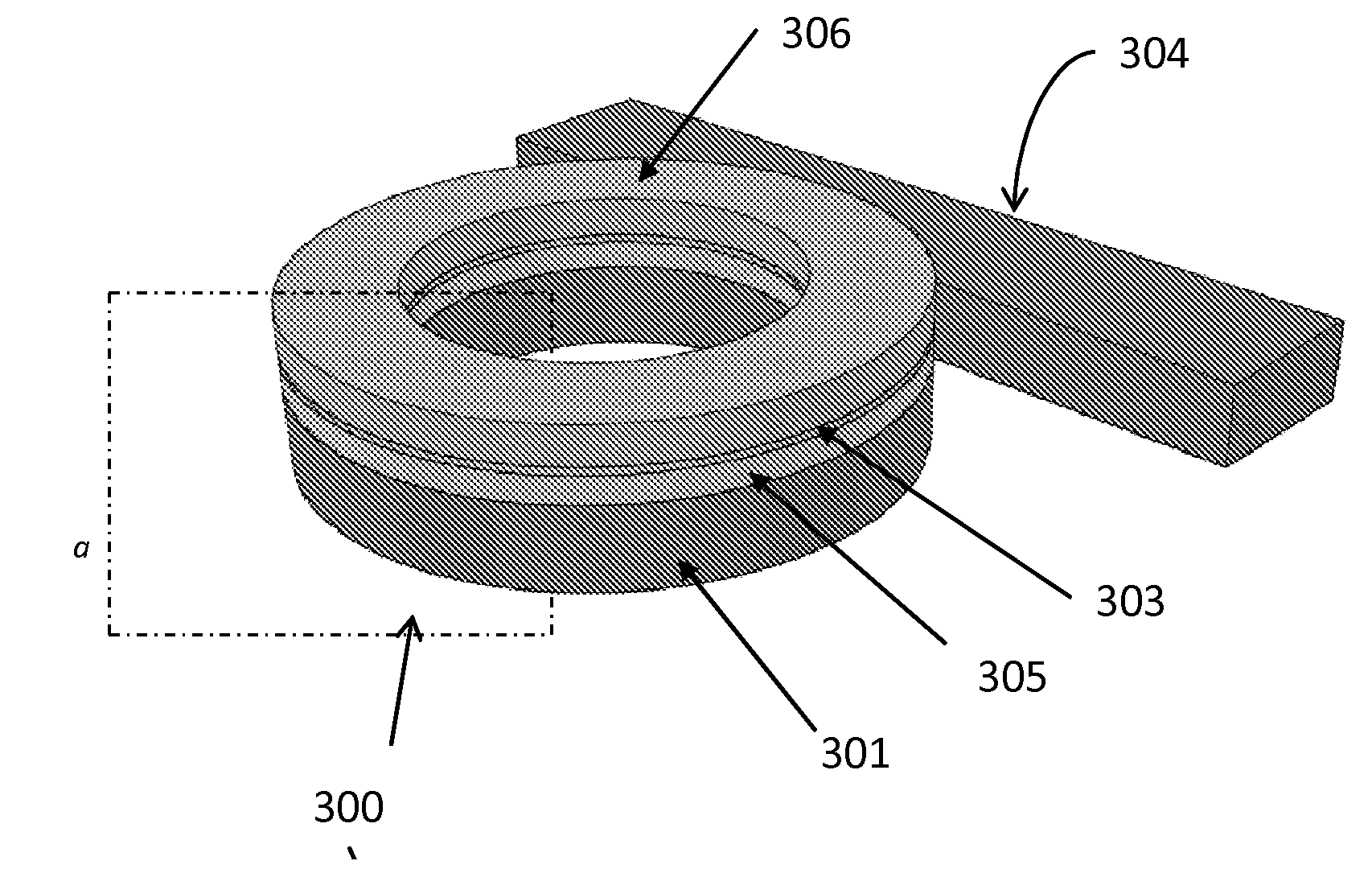
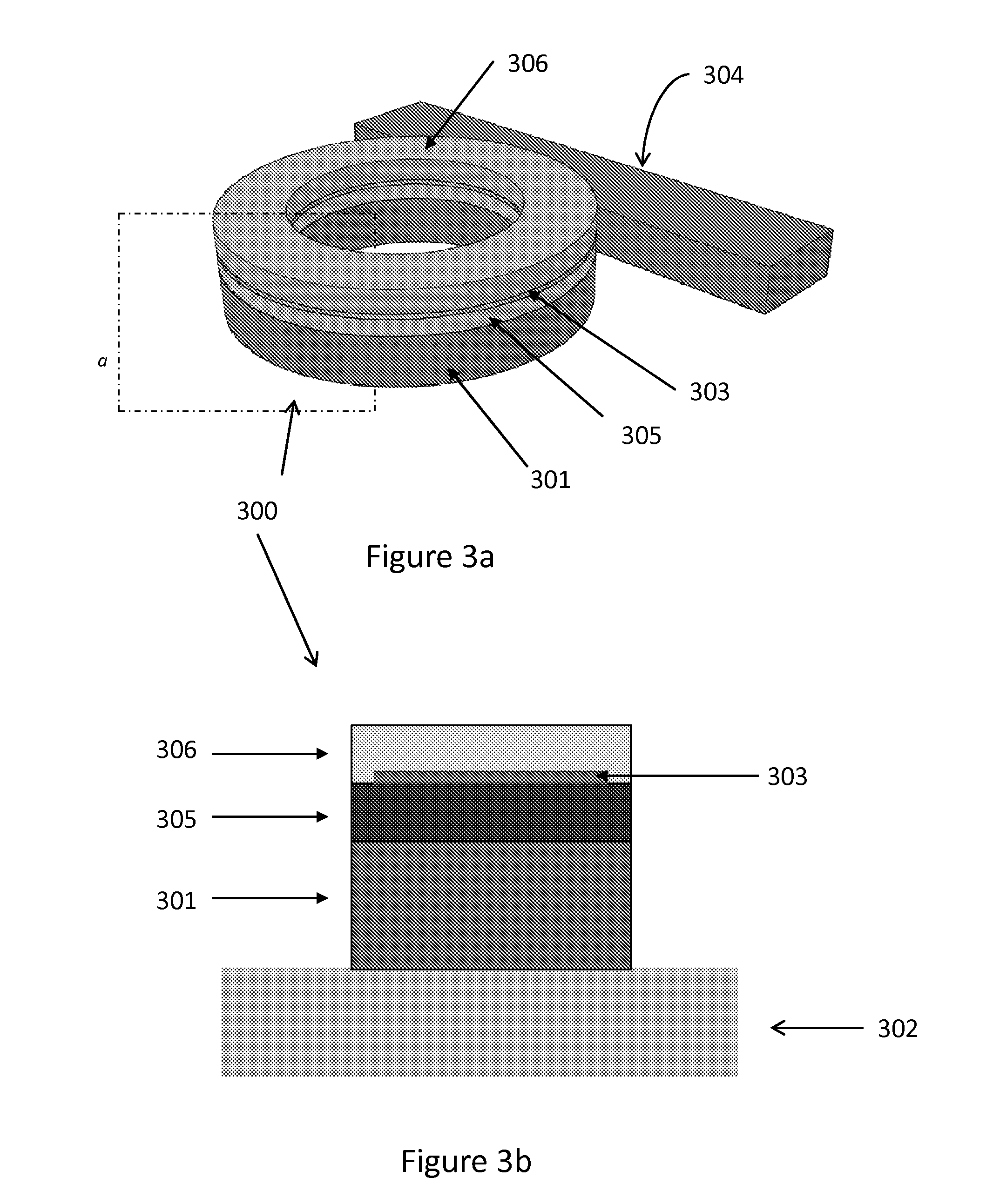
01 Fabrication of silicon micropillars
Silicon micropillars can be fabricated using various techniques such as etching, lithography, and deposition processes. These structures have applications in microelectronics, photonics, and sensors due to their unique properties and controllable dimensions.- Fabrication methods for silicon micropillars: Various techniques are employed to create silicon micropillars, including etching processes, lithography, and deposition methods. These fabrication methods allow for precise control over the size, shape, and arrangement of the micropillars, which is crucial for their performance in different applications.
- Applications in solar cells and photovoltaics: Silicon micropillars are utilized in solar cell and photovoltaic technologies to enhance light absorption and improve overall efficiency. The unique structure of micropillars allows for better light trapping and increased surface area, leading to improved energy conversion in solar devices.
- Use in microfluidic and lab-on-a-chip devices: Silicon micropillars play a significant role in microfluidic systems and lab-on-a-chip devices. They can be used for fluid manipulation, particle separation, and as structural elements in miniaturized analytical systems, enabling more efficient and precise microfluidic operations.
- Integration with sensors and MEMS devices: Silicon micropillars are integrated into various sensors and MEMS (Micro-Electro-Mechanical Systems) devices. Their unique properties allow for enhanced sensitivity in chemical and biological sensors, as well as improved performance in mechanical sensing applications.
- Surface modification and functionalization: The surface of silicon micropillars can be modified and functionalized to tailor their properties for specific applications. This includes coating with various materials, chemical treatments, and the addition of functional groups to enhance their performance in areas such as catalysis, sensing, and biomedical applications.
02 Silicon micropillars in solar cells
Silicon micropillars are utilized in solar cell technology to enhance light absorption and improve overall efficiency. The high aspect ratio and surface area of these structures contribute to better photon capture and charge collection.Expand Specific Solutions03 Microfluidic applications of silicon micropillars
Silicon micropillars are employed in microfluidic devices for various purposes, including fluid manipulation, particle separation, and chemical analysis. The precise control over pillar geometry and spacing allows for tailored fluidic behavior.Expand Specific Solutions04 Silicon micropillars in MEMS devices
Micro-electromechanical systems (MEMS) incorporate silicon micropillars for sensing and actuation purposes. These structures can be designed to respond to mechanical, thermal, or electrical stimuli, enabling various applications in consumer electronics and industrial systems.Expand Specific Solutions05 Surface modification of silicon micropillars
The surface of silicon micropillars can be modified to enhance their properties or functionalities. Techniques such as chemical treatment, coating, or functionalization are used to tailor the surface characteristics for specific applications, including improved wettability or biocompatibility.Expand Specific Solutions
Key Players in Plasmonic Technology
The use of silicon micropillars in plasmonic devices represents an emerging field at the intersection of nanotechnology and optics. This technology is in its early development stage, with significant research efforts but limited commercial applications. The market size is currently modest but expected to grow as the technology matures. Key players like IBM, Hitachi, and Tokyo Electron are investing in R&D, while academic institutions such as Caltech and ETH Zurich are driving fundamental research. The technology's maturity varies, with some basic principles established but challenges remaining in scalability and integration. Industry-academia collaborations are accelerating progress, indicating a competitive landscape poised for rapid evolution in the coming years.
The Regents of the University of California
Technical Solution: The University of California has developed innovative plasmonic devices utilizing silicon micropillars. Their approach involves creating arrays of silicon micropillars on a substrate, which are then coated with a thin layer of plasmonic material, typically gold or silver. This structure allows for enhanced light-matter interactions at the nanoscale. The micropillars act as waveguides, concentrating electromagnetic fields and enabling strong coupling between incident light and surface plasmons. This design has shown significant improvements in sensitivity for biosensing applications, with reported detection limits in the femtomolar range [1][3]. The university has also explored the use of these structures for solar energy harvesting, demonstrating increased absorption efficiency across a broad spectrum of wavelengths [2].
Strengths: High sensitivity for biosensing, broad spectrum light absorption for solar applications. Weaknesses: Fabrication complexity, potential for higher costs in large-scale production.
California Institute of Technology
Technical Solution: Caltech has pioneered the integration of silicon micropillars with plasmonic nanostructures to create hybrid photonic-plasmonic devices. Their approach involves etching silicon micropillars into a substrate and then selectively depositing plasmonic nanoparticles or nanoantennas on the pillar tips. This configuration allows for precise control over the coupling between photonic modes in the silicon and plasmonic modes in the metal nanostructures. The institute has demonstrated remarkable enhancements in light emission and absorption using these hybrid structures, with reported Purcell factors exceeding 1000 for quantum emitters placed near the plasmonic hot spots [4]. Additionally, Caltech researchers have explored the use of these devices for on-chip optical communication, showing potential for ultra-compact and efficient optical modulators operating at speeds up to 100 GHz [5].
Strengths: Exceptional light-matter interaction enhancement, potential for high-speed optical communication. Weaknesses: Challenges in maintaining consistent quality across large arrays, potential for optical losses in plasmonic components.
Core Innovations in Silicon-Plasmon Interactions
Plasmonic and photonic resonator structures and methods for large electromagnetic field enhancements
PatentInactiveUS20120281957A1
Innovation
- A hybrid plasmonic photonic resonator structure that combines a photonic resonator with a plasmonic resonator, using a photonic waveguide to efficiently couple light to plasmonic nanoparticles, achieving high field enhancement and coupling efficiency through a buffer layer and cladding layer design, allowing for compact and sensitive refractive index sensing.
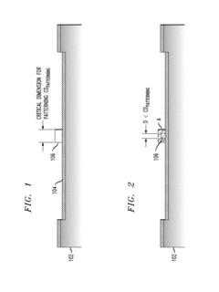
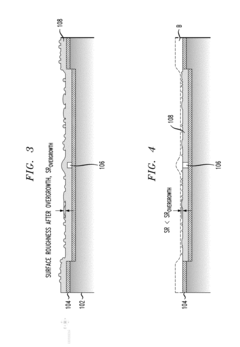
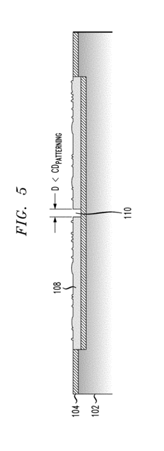
Negative patterning approach for ultra-narrow gap devices
PatentInactiveUS20180057930A1
Innovation
- A method involving the formation of a buried template structure on a substrate, followed by deposition and planarization of an active material layer, and selective removal of the template to create ultra-narrow gaps, allowing for precise control over dimensions and alignment of plasmonic structures with low surface roughness and improved morphology.

Environmental Impact of Plasmonic Device Manufacturing
The manufacturing of plasmonic devices incorporating silicon micropillars presents both environmental challenges and opportunities. The production process involves several stages that can have significant ecological impacts, including material extraction, fabrication, and waste management.
Silicon, the primary material for micropillars, is abundant in nature but requires energy-intensive mining and purification processes. The extraction of high-purity silicon for semiconductor applications often involves the use of hazardous chemicals and generates substantial carbon emissions. However, the semiconductor industry has made strides in recent years to improve the efficiency of silicon production and reduce its environmental footprint.
The fabrication of silicon micropillars typically employs advanced lithography and etching techniques. These processes require cleanroom environments, which consume large amounts of energy for maintaining precise temperature and humidity controls. Additionally, the use of photoresists, etchants, and other chemicals in the fabrication process can lead to the generation of hazardous waste that requires careful handling and disposal.
On the positive side, the miniaturization enabled by silicon micropillars in plasmonic devices can lead to more efficient use of materials and energy in the final products. This could potentially offset some of the environmental costs associated with their production. Furthermore, the enhanced performance of plasmonic devices using silicon micropillars may contribute to advancements in fields such as solar energy harvesting and optical sensing, which have broader positive environmental implications.
Water usage is another critical environmental consideration in the manufacturing of these devices. The semiconductor industry is known for its high water consumption, particularly in the cleaning and rinsing stages of production. However, many manufacturers are implementing water recycling systems and exploring waterless cleaning technologies to mitigate this impact.
The end-of-life management of plasmonic devices with silicon micropillars also presents environmental challenges. While silicon itself is not toxic, the complex integration with other materials in plasmonic devices can make recycling difficult. Developing effective recycling and disposal methods for these advanced devices is crucial to minimize their long-term environmental impact.
As the technology matures, there is a growing focus on developing more sustainable manufacturing processes for plasmonic devices. This includes research into alternative materials, more efficient fabrication techniques, and improved waste management strategies. The industry is also exploring the potential of circular economy principles to reduce the overall environmental footprint of these advanced devices throughout their lifecycle.
Standardization Efforts in Plasmonic Device Industry
The standardization efforts in the plasmonic device industry have been gaining momentum in recent years, driven by the need for consistency and interoperability in this rapidly evolving field. As the use of silicon micropillars in plasmonic devices becomes more prevalent, industry stakeholders have recognized the importance of establishing common guidelines and specifications.
Several international organizations have taken the lead in developing standards for plasmonic devices. The International Electrotechnical Commission (IEC) has formed a technical committee dedicated to nanotechnology standardization, which includes a working group focused on plasmonic devices. This group is working on creating a standardized terminology and measurement methods for plasmonic structures, including those incorporating silicon micropillars.
The Institute of Electrical and Electronics Engineers (IEEE) has also been active in this area, with its Photonics Society spearheading efforts to standardize plasmonic device characterization techniques. These efforts aim to establish uniform protocols for measuring key performance parameters of plasmonic devices, such as resonance wavelength, quality factor, and field enhancement.
In the realm of silicon micropillars specifically, the National Institute of Standards and Technology (NIST) has been developing reference materials and measurement protocols. These standards are crucial for ensuring the reproducibility of silicon micropillar fabrication processes and the consistent performance of resulting plasmonic devices across different laboratories and manufacturing facilities.
Industry consortia have also emerged to address standardization needs. The Plasmonic Device Consortium, comprising leading companies and research institutions, is working on creating best practices for the design, fabrication, and testing of plasmonic devices incorporating silicon micropillars. Their efforts include developing standard file formats for device designs and simulation results, as well as establishing quality control benchmarks for manufacturing processes.
Standardization efforts are also focusing on the integration of plasmonic devices with existing photonic and electronic systems. The Photonics Industry and Technology Association (PIDA) is leading initiatives to define interface standards for plasmonic components, ensuring seamless integration with conventional optical and electronic circuits.
As the field continues to mature, these standardization efforts are expected to accelerate, fostering innovation and commercialization of plasmonic devices based on silicon micropillars. The establishment of widely accepted standards will likely lead to improved reliability, reduced costs, and increased adoption of this technology across various industries.
Unlock deeper insights with Patsnap Eureka Quick Research — get a full tech report to explore trends and direct your research. Try now!
Generate Your Research Report Instantly with AI Agent
Supercharge your innovation with Patsnap Eureka AI Agent Platform!