The Use of Silicon Micropillars in Microengineering
JUL 9, 20259 MIN READ
Generate Your Research Report Instantly with AI Agent
Patsnap Eureka helps you evaluate technical feasibility & market potential.
Silicon Micropillars Background and Objectives
Silicon micropillars have emerged as a groundbreaking technology in the field of microengineering, offering unprecedented opportunities for innovation across various industries. These microscopic structures, typically ranging from a few micrometers to several hundred micrometers in height, are fabricated from silicon substrates using advanced etching techniques. The development of silicon micropillars represents a significant milestone in the ongoing miniaturization trend in technology, enabling the creation of highly efficient and compact devices.
The evolution of silicon micropillars can be traced back to the early 2000s when researchers began exploring new ways to enhance the surface area and functionality of silicon-based devices. Initially, the focus was primarily on improving the efficiency of solar cells and enhancing the sensitivity of biosensors. However, as fabrication techniques advanced and the potential applications became more apparent, the scope of silicon micropillar research expanded rapidly.
Today, silicon micropillars are at the forefront of numerous technological advancements, spanning fields such as optoelectronics, microfluidics, and energy harvesting. Their unique properties, including high surface-to-volume ratio, controllable geometry, and compatibility with existing semiconductor manufacturing processes, make them ideal candidates for a wide range of applications. From enhancing the performance of photovoltaic cells to enabling more sensitive chemical and biological sensors, silicon micropillars are revolutionizing the capabilities of microengineered devices.
The primary objectives of silicon micropillar research and development are multifaceted. Firstly, there is a strong focus on optimizing the fabrication processes to achieve greater control over the size, shape, and spacing of the micropillars. This includes refining etching techniques and exploring new methods for creating complex three-dimensional structures. Secondly, researchers aim to expand the functional capabilities of silicon micropillars by incorporating novel materials or modifying their surface properties.
Another key objective is to bridge the gap between laboratory demonstrations and large-scale industrial applications. This involves addressing challenges related to scalability, cost-effectiveness, and integration with existing technologies. Additionally, there is a growing emphasis on exploring the potential of silicon micropillars in emerging fields such as quantum computing and neuromorphic engineering, where their unique properties could enable breakthrough innovations.
As we look to the future, the continued development of silicon micropillars is expected to play a crucial role in advancing miniaturization, enhancing device performance, and enabling new functionalities across a wide spectrum of technological applications. The ongoing research in this field promises to unlock new possibilities in areas ranging from renewable energy to advanced medical diagnostics, solidifying the position of silicon micropillars as a key enabling technology in the era of microengineering.
Market Demand Analysis for Micropillar Applications
The market demand for silicon micropillars in microengineering applications has been steadily growing, driven by the increasing need for miniaturization and enhanced performance in various industries. These microscale structures offer unique advantages in fields such as microfluidics, biosensors, and energy harvesting, leading to a surge in research and development activities.
In the microfluidics sector, silicon micropillars have gained significant traction due to their ability to manipulate and control fluid flow at the microscale level. This has opened up new possibilities for lab-on-a-chip devices, point-of-care diagnostics, and drug delivery systems. The global microfluidics market, which heavily relies on micropillar technology, is expected to experience substantial growth in the coming years.
The biosensor industry has also shown a keen interest in silicon micropillars. These structures provide increased surface area and improved sensitivity for detecting biomolecules, making them ideal for applications in medical diagnostics, environmental monitoring, and food safety. As the demand for rapid and accurate sensing technologies continues to rise, the market for micropillar-based biosensors is projected to expand significantly.
Energy harvesting is another area where silicon micropillars have found promising applications. Their unique properties allow for efficient conversion of mechanical energy into electrical energy, making them suitable for powering small electronic devices and sensors. This aligns well with the growing trend of Internet of Things (IoT) devices and wearable technologies, further driving the demand for micropillar-based energy harvesting solutions.
The semiconductor industry has also recognized the potential of silicon micropillars in improving the performance of electronic devices. These structures can be used to enhance heat dissipation, reduce electrical resistance, and improve overall device efficiency. As the demand for faster and more energy-efficient electronics continues to grow, the market for micropillar-based semiconductor solutions is expected to expand.
In the field of optics and photonics, silicon micropillars have shown promise in creating novel optical devices and sensors. Their ability to manipulate light at the microscale level has led to applications in areas such as optical communications, display technologies, and imaging systems. The increasing demand for high-performance optical components is likely to drive further growth in this sector.
While the market demand for silicon micropillars is growing across various industries, it is important to note that the technology is still in its early stages of commercialization. Many applications are currently in the research and development phase, with potential for significant market expansion as the technology matures and becomes more widely adopted.
Current State and Challenges in Micropillar Fabrication
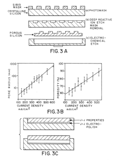
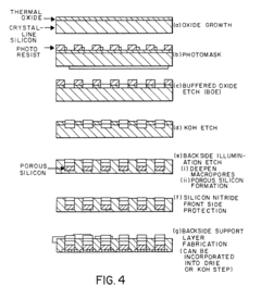
The fabrication of silicon micropillars has seen significant advancements in recent years, driven by their potential applications in various microengineering fields. Currently, the most common methods for producing these structures include photolithography, electron beam lithography, and focused ion beam milling. Each technique offers unique advantages and limitations in terms of resolution, scalability, and cost-effectiveness.
Photolithography remains the most widely used method in industrial settings due to its high throughput and relatively low cost. However, it faces challenges in achieving sub-micron feature sizes, which are increasingly demanded in cutting-edge applications. Electron beam lithography, on the other hand, excels in creating ultra-fine structures but suffers from low throughput and high equipment costs, limiting its use primarily to research and development environments.
One of the major challenges in micropillar fabrication is achieving high aspect ratios while maintaining structural integrity. As the height-to-width ratio increases, issues such as pillar collapse and pattern distortion become more pronounced. This is particularly problematic in applications requiring tall, densely packed micropillars, such as in advanced heat sinks or microfluidic devices.
Material selection and optimization present another significant challenge. While silicon remains the primary material due to its well-established processing techniques and favorable properties, there is growing interest in exploring alternative materials like polymers and metals. Each material brings its own set of fabrication challenges, including etch selectivity, stress management, and surface quality control.
The precise control of micropillar geometry and surface characteristics is crucial for many applications but remains difficult to achieve consistently. Variations in pillar diameter, height, and spacing can significantly impact device performance. Additionally, the sidewall roughness and tip shape of micropillars are critical parameters that are challenging to control at the nanoscale.
Scalability and cost-effectiveness continue to be major hurdles in the widespread adoption of silicon micropillar technology. While laboratory-scale production has demonstrated impressive capabilities, translating these achievements to large-scale manufacturing processes without compromising quality or increasing costs substantially is an ongoing challenge.
Emerging techniques such as nanoimprint lithography and self-assembly methods show promise in addressing some of these challenges. These approaches offer potential solutions for high-throughput, cost-effective production of nanostructured surfaces. However, they are still in the early stages of development and face their own set of technical hurdles, particularly in achieving the precision and reproducibility required for commercial applications.
Existing Micropillar Fabrication Techniques
01 Fabrication methods for silicon micropillars
Various techniques are employed to create silicon micropillars, including etching processes, lithography, and deposition methods. These fabrication methods allow for precise control over the size, shape, and arrangement of the micropillars, which is crucial for their performance in different applications.- Fabrication methods for silicon micropillars: Various techniques are employed to create silicon micropillars, including etching processes, lithography, and deposition methods. These fabrication methods allow for precise control over the size, shape, and arrangement of the micropillars, which is crucial for their performance in different applications.
- Applications in solar cells and photovoltaics: Silicon micropillars are utilized in solar cell and photovoltaic technologies to enhance light absorption and improve overall efficiency. The unique structure of micropillars allows for better light trapping and increased surface area, leading to improved energy conversion rates.
- Use in microfluidic and lab-on-a-chip devices: Silicon micropillars play a significant role in microfluidic systems and lab-on-a-chip devices. They can be used for fluid manipulation, particle separation, and as supports for various chemical and biological reactions, enhancing the functionality of these miniaturized systems.
- Integration with sensors and MEMS devices: Silicon micropillars are integrated into various sensors and MEMS (Micro-Electro-Mechanical Systems) devices. Their unique properties allow for enhanced sensitivity, improved signal-to-noise ratios, and increased functionality in applications such as pressure sensors, accelerometers, and chemical detectors.
- Surface modification and functionalization: The surface of silicon micropillars can be modified and functionalized to tailor their properties for specific applications. This includes coating with various materials, chemical treatments, and the addition of functional groups to enhance their performance in areas such as catalysis, sensing, and biomedical applications.
02 Applications in solar cells and photovoltaics
Silicon micropillars are utilized in solar cell and photovoltaic technologies to enhance light absorption and improve overall efficiency. The unique structure of micropillars allows for better light trapping and increased surface area, leading to improved energy conversion in solar devices.Expand Specific Solutions03 Use in microfluidic and lab-on-a-chip devices
Silicon micropillars play a significant role in microfluidic systems and lab-on-a-chip devices. They can be used for fluid manipulation, particle separation, and as structural elements in miniaturized analytical systems, enabling more efficient and precise biomedical and chemical analyses.Expand Specific Solutions04 Integration with MEMS and sensor technologies
Silicon micropillars are integrated into Micro-Electro-Mechanical Systems (MEMS) and various sensor technologies. Their unique properties allow for the development of highly sensitive and miniaturized sensors for applications in environmental monitoring, biomedical devices, and industrial process control.Expand Specific Solutions05 Surface modification and functionalization
The surface of silicon micropillars can be modified and functionalized to enhance their properties or add new functionalities. This includes coating with various materials, chemical treatments, or attaching specific molecules to tailor the micropillars for particular applications such as biosensing or catalysis.Expand Specific Solutions
Key Players in Microengineering Industry
The use of silicon micropillars in microengineering is an emerging field with significant potential. The market is in its early growth stage, characterized by increasing research activities and pilot applications. While the market size is still relatively small, it is expected to expand rapidly as the technology matures. Companies like Shanghai Institute of Microsystem & Information Technology, NXP Semiconductors, and STMicroelectronics are at the forefront of developing this technology. Universities such as Zhejiang University and Portland State University are contributing to fundamental research. The involvement of major players like IBM and Xerox indicates growing industry interest. However, the technology is still in the development phase, with ongoing efforts to improve fabrication processes and explore new applications.
Shanghai Institute of Microsystem & Information Technology
Technical Solution: The Shanghai Institute of Microsystem & Information Technology (SIMIT) has developed advanced techniques for fabricating silicon micropillars using deep reactive ion etching (DRIE). Their approach allows for the creation of high aspect ratio structures with precise control over pillar dimensions and spacing. SIMIT has demonstrated the use of these micropillars in various microengineering applications, including microfluidic devices, sensors, and energy harvesting systems. Their research has shown that silicon micropillars can significantly enhance surface area and improve heat transfer efficiency in microscale devices [1][3]. SIMIT has also explored the use of micropillars for anti-reflective coatings and light trapping in photovoltaic cells, achieving up to 15% improvement in light absorption [2].
Strengths: Expertise in DRIE fabrication, ability to create high aspect ratio structures, diverse applications in microfluidics and sensors. Weaknesses: Potential scalability issues for mass production, limited to silicon-based materials.
International Business Machines Corp.
Technical Solution: IBM has made significant strides in the use of silicon micropillars for microengineering applications, particularly in the field of microelectronics and chip cooling. Their research has focused on developing dense arrays of silicon micropillars to enhance heat dissipation in high-performance computing systems. IBM's approach involves creating micropillar structures with optimized geometries and surface treatments to maximize thermal conductivity and fluid flow. They have demonstrated cooling efficiency improvements of up to 30% compared to traditional heat sink designs [4]. Additionally, IBM has explored the use of silicon micropillars in 3D chip stacking technologies, where the pillars serve as both structural supports and electrical interconnects, enabling higher integration densities and improved signal transmission [5].
Strengths: Strong focus on thermal management applications, integration with existing semiconductor manufacturing processes. Weaknesses: Primarily centered on computing applications, may have limited versatility in other fields.
Core Innovations in Silicon Micropillar Design
Micro-pillar assisted semiconductor bonding
PatentActiveUS20150364441A1
Innovation
- The use of micro pillars on the silicon substrate to penetrate and break indium oxide, reducing the initial surface contact area and heat transfer, allowing for easier melting of indium and improved bonding by modulating heat and pressure transfer.
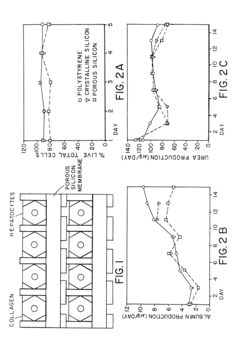
Nanoporous silicon support containing macropores for use as a bioreactor
PatentInactiveUS6734000B2
Innovation
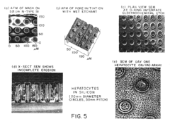
- A nanoporous silicon bioreactor is developed, featuring macropores of defined sizes to accommodate cells and nanopores for media passage, allowing for the integration of biosensors and enhanced surface area, which supports the growth and differentiation of primary hepatocytes and other cell types, enabling pseudo-3D interactions and bidirectional mass transfer.
Environmental Impact of Micropillar Production
The production of silicon micropillars in microengineering has significant environmental implications that warrant careful consideration. The manufacturing process involves several stages, each with its own environmental impact. The primary raw material, silicon, is abundant in nature but requires energy-intensive extraction and purification processes. The mining and refining of silicon can lead to habitat disruption, soil erosion, and water pollution if not managed properly.
The fabrication of micropillars typically employs techniques such as photolithography and etching, which involve the use of various chemicals and gases. These processes can generate hazardous waste materials, including spent etchants and photoresist residues. Proper disposal and treatment of these wastes are crucial to prevent soil and water contamination. Additionally, the clean room environments required for micropillar production consume substantial amounts of energy for maintaining precise temperature, humidity, and air quality conditions.
Water usage is another significant environmental concern in micropillar production. The manufacturing process requires large volumes of ultra-pure water for cleaning and rinsing steps. The purification and subsequent treatment of this water contribute to the overall environmental footprint of the production process. Furthermore, the potential for water pollution through the release of contaminated effluents must be carefully managed.
The energy consumption associated with micropillar production extends beyond the manufacturing process itself. The operation of sophisticated equipment, such as electron microscopes and plasma etchers, demands considerable electrical power. This energy demand indirectly contributes to greenhouse gas emissions, depending on the source of electricity used in the production facilities.
However, it is important to note that the environmental impact of micropillar production should be balanced against the potential benefits of their applications. Micropillars can enhance the efficiency of various devices, including solar cells and sensors, which may lead to overall environmental benefits in terms of energy conservation and resource utilization.
As the field of microengineering advances, there is a growing focus on developing more sustainable production methods for micropillars. Research is being conducted on alternative materials, more efficient fabrication techniques, and improved waste management strategies. These efforts aim to reduce the environmental footprint of micropillar production while maintaining or enhancing their functional properties.
Scalability and Cost Analysis
The scalability and cost analysis of silicon micropillars in microengineering reveals both promising opportunities and significant challenges. As the demand for miniaturized devices continues to grow across various industries, the ability to scale up production of silicon micropillars becomes increasingly crucial.
One of the primary advantages of silicon micropillars is their potential for mass production using existing semiconductor fabrication techniques. This compatibility with established manufacturing processes offers a pathway for scalability. However, the precision required in creating uniform arrays of micropillars at nanoscale dimensions presents technical hurdles that impact both scalability and cost.
The initial capital investment for setting up production facilities capable of manufacturing silicon micropillars at scale is substantial. This includes the cost of specialized equipment such as advanced lithography systems, etching tools, and metrology instruments. While these costs can be amortized over large production volumes, they represent a significant barrier to entry for smaller companies or research institutions.
Material costs for high-purity silicon wafers used in micropillar fabrication are relatively low compared to other components in microengineering. However, the processing steps required to create micropillars, including precise patterning and etching, contribute significantly to the overall production expenses. As production scales up, opportunities for cost reduction through process optimization and automation become available.
The yield rate in micropillar production is a critical factor affecting both scalability and cost-effectiveness. Achieving consistent quality and uniformity across large arrays of micropillars remains challenging, particularly as the dimensions decrease. Improvements in process control and defect reduction are essential for enhancing yield and reducing per-unit costs as production scales.
Energy consumption during the fabrication process is another consideration in cost analysis. The high-temperature processes and vacuum environments required for silicon micropillar production contribute to operational expenses. As production scales up, investments in energy-efficient equipment and processes can lead to long-term cost savings.
The potential for economies of scale in silicon micropillar production is significant. As manufacturing volumes increase, the per-unit cost is expected to decrease due to improved process efficiency, better resource utilization, and the distribution of fixed costs over larger production runs. This trend makes silicon micropillars increasingly attractive for applications in various fields, including sensors, microfluidics, and energy harvesting devices.
Unlock deeper insights with Patsnap Eureka Quick Research — get a full tech report to explore trends and direct your research. Try now!
Generate Your Research Report Instantly with AI Agent
Supercharge your innovation with Patsnap Eureka AI Agent Platform!