Silicon Micropillars and Nanoantennas: A Synergistic Relationship
JUL 9, 20259 MIN READ
Generate Your Research Report Instantly with AI Agent
Patsnap Eureka helps you evaluate technical feasibility & market potential.
Silicon Micropillars and Nanoantennas Synergy Overview
The synergistic relationship between Silicon Micropillars and Nanoantennas represents a cutting-edge area of research in the field of nanophotonics and optoelectronics. This innovative combination leverages the unique properties of both structures to enhance light-matter interactions and improve device performance in various applications.
Silicon micropillars, typically ranging from a few micrometers to tens of micrometers in height, offer excellent light trapping capabilities and increased surface area. These structures have been extensively studied for their potential in photovoltaics, sensors, and light-emitting devices. The high aspect ratio and controllable dimensions of micropillars allow for efficient light absorption and emission across a broad spectrum.
Nanoantennas, on the other hand, are metallic or dielectric nanostructures designed to efficiently couple light from free space into nanoscale volumes. They can concentrate electromagnetic energy into subwavelength regions, enhancing local field intensities and modifying the emission properties of nearby emitters. Nanoantennas have shown promise in applications such as surface-enhanced spectroscopy, photon upconversion, and quantum optics.
The synergy between silicon micropillars and nanoantennas arises from their complementary functionalities. By integrating nanoantennas onto the surface or within the structure of silicon micropillars, researchers can create hybrid systems that combine the light-trapping effects of micropillars with the near-field enhancement capabilities of nanoantennas.
This synergistic approach offers several advantages. First, it allows for more efficient light coupling into the micropillar structure, potentially increasing absorption or emission efficiency. Second, the enhanced local fields generated by nanoantennas can boost light-matter interactions within the silicon material, leading to improved device performance.
Furthermore, the combination enables novel device architectures that can exploit both far-field and near-field optical effects. For instance, in photovoltaic applications, micropillars can provide broadband light trapping, while strategically placed nanoantennas can enhance absorption at specific wavelengths or in targeted regions of the device.
The research in this area focuses on optimizing the design, fabrication, and integration of these two components. Key challenges include achieving precise control over nanoantenna placement and orientation on the micropillar surfaces, ensuring compatibility of fabrication processes, and understanding the complex electromagnetic interactions in these hybrid systems.
As this field continues to evolve, it promises to unlock new possibilities in optoelectronic device design, potentially leading to more efficient solar cells, ultra-sensitive sensors, and novel quantum optical devices. The synergy between silicon micropillars and nanoantennas exemplifies the power of combining different nanostructures to create systems with enhanced functionality and performance.
Market Potential for Integrated Photonic Devices
The integration of silicon micropillars and nanoantennas in photonic devices presents a significant market opportunity in the rapidly evolving field of integrated photonics. This synergistic combination addresses key challenges in optical communication, sensing, and computing, potentially revolutionizing various industries.
The market for integrated photonic devices is experiencing robust growth, driven by increasing demand for high-speed data transmission, efficient computing, and advanced sensing technologies. The global integrated photonics market is expected to expand substantially over the next decade, with applications spanning telecommunications, data centers, healthcare, and automotive sectors.
In telecommunications, the integration of silicon micropillars and nanoantennas can enhance the performance of optical transceivers, enabling higher data rates and improved energy efficiency. This technology is crucial for meeting the growing bandwidth demands of 5G and future 6G networks. Data centers, another key market segment, can benefit from reduced power consumption and increased data processing capabilities offered by these advanced photonic devices.
The healthcare industry presents a promising market for integrated photonic devices incorporating silicon micropillars and nanoantennas. These components can be utilized in biosensors for rapid and sensitive disease detection, as well as in advanced imaging systems for medical diagnostics. The potential for miniaturization and increased sensitivity makes this technology particularly attractive for point-of-care applications and wearable health monitoring devices.
In the automotive sector, the synergy between silicon micropillars and nanoantennas can enhance LiDAR systems, crucial for autonomous vehicles. The improved light manipulation and detection capabilities offered by this combination can lead to more accurate and efficient sensing systems, accelerating the development and adoption of self-driving technologies.
The industrial automation and smart manufacturing sectors also stand to benefit from integrated photonic devices. Enhanced sensors and communication systems based on this technology can improve process control, quality assurance, and overall operational efficiency in manufacturing environments.
As the Internet of Things (IoT) continues to expand, the demand for compact, energy-efficient sensors and communication devices grows. Integrated photonic devices leveraging silicon micropillars and nanoantennas are well-positioned to meet these requirements, offering potential applications in smart cities, environmental monitoring, and agriculture.
The market potential for this technology extends to quantum computing and communications. The ability to manipulate light at the nanoscale opens up possibilities for quantum information processing and secure communication systems, areas that are attracting significant investment and research interest globally.
Current Challenges in Micropillar-Nanoantenna Integration
The integration of silicon micropillars and nanoantennas presents several significant challenges that researchers and engineers must overcome to fully harness the synergistic potential of these two technologies. One of the primary obstacles is achieving precise alignment and positioning of nanoantennas on micropillar structures. The nanoscale dimensions of both components require extremely high precision in fabrication and assembly processes, which can be difficult to achieve consistently at scale.
Another challenge lies in maintaining the optical and electrical properties of both the micropillars and nanoantennas during integration. The fabrication processes for each component may involve different materials and techniques, potentially leading to compatibility issues. For instance, the high-temperature processes often used in silicon micropillar fabrication could potentially damage or alter the properties of pre-existing nanoantennas.
The optimization of the interface between micropillars and nanoantennas poses yet another hurdle. Ensuring efficient energy transfer and coupling between these structures is crucial for maximizing their synergistic effects. This requires careful engineering of the contact area and consideration of factors such as surface roughness, material composition, and potential interfacial layers.
Scalability and cost-effectiveness of production remain significant challenges in micropillar-nanoantenna integration. While laboratory-scale demonstrations have shown promising results, translating these into large-scale, commercially viable manufacturing processes is a complex task. The need for specialized equipment and precise control over nanoscale features can lead to high production costs and low throughput.
Furthermore, the long-term stability and reliability of integrated micropillar-nanoantenna systems are areas of concern. Environmental factors such as temperature fluctuations, humidity, and mechanical stress can potentially degrade the performance or physical integrity of these delicate structures over time. Developing robust protection and packaging solutions without compromising the functionality of the integrated system is a critical challenge.
The characterization and testing of integrated micropillar-nanoantenna systems also present unique difficulties. Traditional measurement techniques may not be suitable for accurately assessing the performance of these complex, multi-scale structures. New metrology methods and standards may need to be developed to properly evaluate and optimize these integrated systems.
Lastly, the multidisciplinary nature of micropillar-nanoantenna integration poses challenges in terms of knowledge integration and collaboration. Expertise from fields such as materials science, nanophotonics, semiconductor physics, and manufacturing engineering must be effectively combined to address the various aspects of this technology. Bridging the gaps between these disciplines and fostering effective communication and collaboration among researchers and engineers from different backgrounds is essential for overcoming the current challenges and advancing the field.
Existing Micropillar-Nanoantenna Coupling Techniques
01 Fabrication of silicon micropillars and nanoantennas
Advanced manufacturing techniques are employed to create silicon micropillars and nanoantennas. These structures are typically fabricated using methods such as lithography, etching, and deposition processes. The precise control of dimensions and shapes at the micro and nanoscale allows for the creation of structures with specific optical and electronic properties.- Fabrication of silicon micropillars and nanoantennas: Advanced manufacturing techniques are employed to create silicon micropillars and nanoantennas. These structures are typically fabricated using methods such as lithography, etching, and deposition processes. The precise control of dimensions and shapes at the micro and nanoscale allows for the creation of structures with specific optical and electronic properties.
- Applications in photovoltaics and solar cells: Silicon micropillars and nanoantennas are utilized in photovoltaic devices and solar cells to enhance light absorption and improve energy conversion efficiency. These structures can manipulate light at the nanoscale, trapping and concentrating it to increase the overall performance of solar energy harvesting systems.
- Integration with optical and sensing devices: Micropillars and nanoantennas are integrated into various optical and sensing devices to enhance their performance. These structures can be used to manipulate light, improve signal detection, and increase sensitivity in applications such as spectroscopy, imaging, and biosensing.
- Electromagnetic field enhancement and manipulation: Silicon micropillars and nanoantennas are designed to enhance and manipulate electromagnetic fields at the micro and nanoscale. This property is exploited in applications such as surface-enhanced spectroscopy, near-field optical microscopy, and plasmonic devices for improved light-matter interactions.
- Integration with MEMS and NEMS devices: Silicon micropillars and nanoantennas are incorporated into Micro-Electro-Mechanical Systems (MEMS) and Nano-Electro-Mechanical Systems (NEMS) to enhance their functionality. These structures can be used for actuation, sensing, and signal transduction in miniaturized devices for various applications in electronics, telecommunications, and biomedical fields.
02 Applications in photovoltaics and solar cells
Silicon micropillars and nanoantennas are utilized in photovoltaic devices and solar cells to enhance light absorption and improve energy conversion efficiency. These structures can manipulate light at the nanoscale, trapping and concentrating sunlight to increase the overall performance of solar energy harvesting systems.Expand Specific Solutions03 Integration with optical and sensing devices
Micropillars and nanoantennas are incorporated into various optical and sensing devices to enhance their performance. These structures can be used to manipulate light, improve signal detection, and increase sensitivity in applications such as spectroscopy, imaging, and biosensing.Expand Specific Solutions04 Electromagnetic field enhancement and manipulation
Silicon micropillars and nanoantennas are designed to enhance and manipulate electromagnetic fields at the micro and nanoscale. This property is exploited in applications such as surface-enhanced spectroscopy, near-field optical microscopy, and plasmonic devices, enabling improved sensitivity and resolution in various analytical and imaging techniques.Expand Specific Solutions05 Integration with MEMS and NEMS devices
Silicon micropillars and nanoantennas are integrated with Micro-Electro-Mechanical Systems (MEMS) and Nano-Electro-Mechanical Systems (NEMS) to create advanced devices with enhanced functionalities. These structures can be used to improve the performance of sensors, actuators, and other miniaturized systems in fields such as telecommunications, biomedical engineering, and environmental monitoring.Expand Specific Solutions
Key Players in Silicon Photonics Industry
The research on the synergistic relationship between Silicon Micropillars and Nanoantennas is in an emerging stage, with growing interest from academia and industry. The market size is expanding as potential applications in photonics, sensing, and energy harvesting become apparent. While still evolving, the technology shows promise, with key players like California Institute of Technology, IBM, and Xiamen University making significant contributions. The field's relative immaturity presents opportunities for innovation and collaboration among research institutions and companies to advance the technology towards practical applications and commercialization.
California Institute of Technology
Technical Solution: Caltech's research on Silicon Micropillars and Nanoantennas focuses on enhancing light-matter interactions at the nanoscale. They have developed a novel approach combining silicon micropillars with plasmonic nanoantennas to achieve strong coupling between quantum emitters and optical modes[1]. This synergistic relationship allows for precise control over light emission and absorption, potentially revolutionizing applications in quantum optics and photonics. Their method involves fabricating silicon micropillars with embedded quantum dots and integrating them with carefully designed gold nanoantennas[2]. This configuration enables the manipulation of light at subwavelength scales, leading to enhanced spontaneous emission rates and improved light extraction efficiency[3].
Strengths: Cutting-edge research in quantum optics, potential for breakthrough applications in quantum computing and communications. Weaknesses: Complex fabrication process, challenges in scaling up for commercial applications.
International Business Machines Corp.
Technical Solution: IBM's approach to Silicon Micropillars and Nanoantennas research focuses on integrating these technologies into their advanced computing systems. They have developed a hybrid platform that combines silicon micropillars with plasmonic nanoantennas to enhance on-chip optical communication[4]. This synergistic relationship allows for improved light manipulation and routing at the nanoscale, potentially increasing data transfer rates and reducing power consumption in their high-performance computing systems. IBM's technique involves fabricating silicon micropillars with precise dimensions and integrating them with gold nanoantennas, optimized for specific wavelengths used in optical communications[5]. This configuration enables efficient coupling between electronic and photonic components, paving the way for faster and more energy-efficient data processing in next-generation computing architectures[6].
Strengths: Strong integration potential with existing semiconductor technologies, immediate applications in high-performance computing. Weaknesses: Challenges in mass production, potential high costs for initial implementation.
Breakthrough Technologies in Photonic Integration
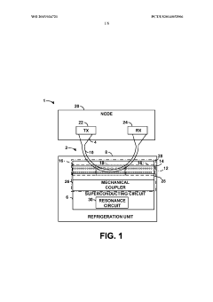
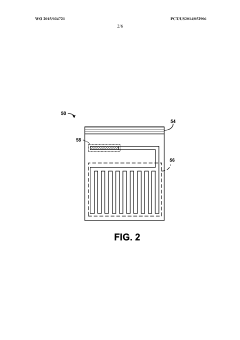
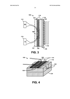
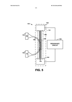
Optical-microwave-quantum transducer
PatentWO2015034721A1
Innovation
- An optical-microwave-quantum transducer is developed, incorporating a tapered optical fiber and a nanophotonic crystal cantilever with a mechanical coupler, which converts optical pulses into mechanical energy, inducing electrical modulation in a superconducting circuit, and vice versa, utilizing electromagnetic and mechanical modes for reversible transduction.
Methods and compositions for enhanced cellular selectivity using nanocarrier-associated ligands
PatentWO2015095866A1
Innovation
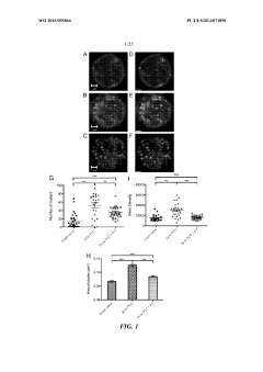
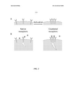
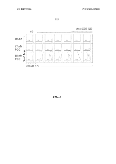
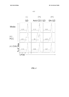
- The use of nanocarrier-associated ligands that bind specifically to microclustered receptors on antigen-experienced cells, enhancing their activation while minimizing activation of naive cells, using nanoparticles such as lipid or polymeric nanoparticles to deliver ligands like anti-CD3 or anti-PD-1 antibodies.
Fabrication Processes for Hybrid Photonic Structures
The fabrication of hybrid photonic structures combining silicon micropillars and nanoantennas requires a sophisticated and multi-step process. This integration leverages the strengths of both components to create advanced photonic devices with enhanced functionalities.
The process typically begins with the fabrication of silicon micropillars on a silicon substrate. This is often achieved through a combination of lithography and etching techniques. Electron beam lithography (EBL) is commonly used to define the precise patterns of the micropillars due to its high resolution. Following pattern definition, reactive ion etching (RIE) or deep reactive ion etching (DRIE) is employed to create the vertical structures of the micropillars.
Once the silicon micropillars are formed, the next step involves the integration of nanoantennas. This can be accomplished through various methods, depending on the specific design requirements. One approach is to use electron beam evaporation or sputtering to deposit a thin layer of plasmonic material, such as gold or silver, onto the silicon structure. This layer is then patterned using EBL followed by lift-off or etching processes to create the nanoantenna structures.
Alternatively, a bottom-up approach can be utilized, where colloidal nanoparticles are synthesized separately and then selectively placed on the silicon micropillars. This method often involves surface functionalization of the micropillars to promote adhesion of the nanoparticles in specific locations.
For more complex designs, multi-layer fabrication techniques may be necessary. This could involve repeated cycles of deposition, lithography, and etching to create three-dimensional hybrid structures with precise control over the positioning of both micropillars and nanoantennas.
Throughout the fabrication process, careful consideration must be given to maintaining the structural integrity and optical properties of both the silicon micropillars and the nanoantennas. This often requires precise control of process parameters such as temperature, pressure, and deposition rates.
Post-fabrication treatments, such as thermal annealing or surface passivation, may be employed to enhance the performance and stability of the hybrid structures. These steps can help reduce defects, improve optical quality, and protect the structures from environmental degradation.
Quality control and characterization are crucial aspects of the fabrication process. Techniques such as scanning electron microscopy (SEM), atomic force microscopy (AFM), and optical spectroscopy are used to verify the dimensions, morphology, and optical properties of the fabricated structures.
Applications in Quantum Computing and Sensing
The synergistic relationship between Silicon Micropillars and Nanoantennas presents exciting opportunities for applications in quantum computing and sensing. This integration of technologies offers enhanced control and manipulation of quantum states, potentially revolutionizing the field of quantum information processing.
In quantum computing, the combination of Silicon Micropillars and Nanoantennas can significantly improve qubit coherence times and fidelity. Silicon Micropillars provide an ideal platform for hosting spin qubits, offering long coherence times due to the low nuclear spin content of isotopically purified silicon. Nanoantennas, when strategically placed near these qubits, can enhance the interaction between light and matter, facilitating more efficient optical readout and control of quantum states.
The enhanced light-matter interaction enabled by this synergistic relationship also allows for more precise quantum sensing applications. Nanoantennas can concentrate electromagnetic fields into subwavelength volumes, dramatically increasing the sensitivity of quantum sensors based on nitrogen-vacancy (NV) centers or other defect-based qubits in silicon.
In the realm of quantum communication, the integration of Silicon Micropillars and Nanoantennas can lead to more efficient quantum repeaters. The micropillars can serve as quantum memories, while the nanoantennas can enhance the emission and collection of single photons, crucial for long-distance quantum information transfer.
For quantum metrology, this synergistic relationship enables the development of ultra-sensitive quantum sensors. The combination can be used to create highly localized and intense electromagnetic fields, allowing for precise measurements of magnetic fields, electric fields, or temperature at the nanoscale.
The scalability of silicon-based technologies makes this approach particularly promising for large-scale quantum systems. The ability to fabricate both Silicon Micropillars and Nanoantennas using established semiconductor manufacturing techniques offers a path towards integrated quantum devices that can be produced at scale.
Furthermore, this synergistic relationship opens up possibilities for hybrid quantum systems. By combining the strengths of both solid-state qubits (in Silicon Micropillars) and photonic qubits (manipulated by Nanoantennas), researchers can explore new paradigms in quantum information processing that leverage the advantages of both approaches.
As research in this area progresses, we can anticipate breakthroughs in quantum error correction, quantum simulation, and the development of practical quantum algorithms. The enhanced control and readout capabilities provided by this synergistic relationship may lead to quantum computers that can outperform classical computers in solving specific problems, bringing us closer to the realization of quantum supremacy in practical applications.
Unlock deeper insights with Patsnap Eureka Quick Research — get a full tech report to explore trends and direct your research. Try now!
Generate Your Research Report Instantly with AI Agent
Supercharge your innovation with Patsnap Eureka AI Agent Platform!