Experimental Techniques for Analyzing Silicon Micropillars
JUL 9, 20259 MIN READ
Generate Your Research Report Instantly with AI Agent
Patsnap Eureka helps you evaluate technical feasibility & market potential.
Silicon Micropillar Analysis Background and Objectives
Silicon micropillars have emerged as a crucial area of study in the field of semiconductor technology and materials science. These nanoscale structures, typically ranging from a few nanometers to several micrometers in diameter, have garnered significant attention due to their unique properties and potential applications in various domains, including electronics, photonics, and energy harvesting.
The development of silicon micropillars can be traced back to the early 2000s when researchers began exploring ways to enhance the performance of silicon-based devices beyond traditional planar structures. The primary objective of studying silicon micropillars is to leverage their high surface-to-volume ratio, enhanced light trapping capabilities, and improved charge carrier dynamics to overcome limitations in conventional silicon technologies.
Over the past two decades, the field has witnessed remarkable progress in fabrication techniques, characterization methods, and theoretical understanding of silicon micropillar behavior. Researchers have explored various approaches to create these structures, including top-down etching processes and bottom-up growth methods, each offering distinct advantages and challenges.
The analysis of silicon micropillars encompasses a wide range of experimental techniques aimed at elucidating their structural, optical, electrical, and mechanical properties. These techniques have evolved significantly, driven by advancements in microscopy, spectroscopy, and nanoscale measurement tools. The primary goals of silicon micropillar analysis include optimizing their geometry, understanding their growth mechanisms, and investigating their interaction with light and charge carriers.
One of the key objectives in this field is to develop precise and reproducible fabrication methods that allow for control over micropillar dimensions, spacing, and surface properties. This is crucial for tailoring the structures to specific applications and ensuring consistent performance across large arrays of micropillars.
Another important aspect of silicon micropillar research is the exploration of their potential in next-generation solar cells, photodetectors, and sensors. By manipulating the size, shape, and arrangement of micropillars, researchers aim to enhance light absorption, reduce reflection losses, and improve charge collection efficiency in photovoltaic devices.
Furthermore, the study of silicon micropillars extends to their integration with other materials and structures, such as quantum dots, plasmonic nanoparticles, and two-dimensional materials. This interdisciplinary approach opens up new avenues for creating hybrid devices with enhanced functionalities and performance characteristics.
As the field continues to evolve, researchers are focusing on developing more sophisticated experimental techniques for analyzing silicon micropillars at the nanoscale. These efforts are driven by the need to gain deeper insights into the fundamental physics governing micropillar behavior and to address challenges in scaling up production for commercial applications.
Market Demand for Silicon Micropillar Applications
The market demand for silicon micropillar applications has been steadily growing across various industries, driven by the unique properties and versatility of these nanostructures. Silicon micropillars offer exceptional mechanical, optical, and electrical characteristics, making them highly attractive for a wide range of applications.
In the semiconductor industry, silicon micropillars are increasingly sought after for their potential to enhance the performance of integrated circuits and microelectronic devices. The demand is particularly strong in the development of next-generation transistors, where micropillars can be utilized to create vertical field-effect transistors (VFETs) with improved current density and reduced power consumption. This application is crucial for meeting the ever-increasing demands for faster and more energy-efficient electronic devices.
The photovoltaic sector has also shown significant interest in silicon micropillar technology. Solar cell manufacturers are exploring the use of micropillars to improve light trapping and absorption, potentially leading to higher efficiency solar panels. The textured surface created by micropillars can significantly reduce reflection and increase the path length of light within the cell, thereby boosting overall energy conversion efficiency.
In the field of sensors and detectors, silicon micropillars are gaining traction due to their high surface-to-volume ratio and customizable geometries. This makes them ideal for applications in chemical and biological sensing, where increased sensitivity and specificity are paramount. The market for such advanced sensors is expanding rapidly, driven by demands in healthcare, environmental monitoring, and industrial process control.
The biomedical industry is another sector showing growing interest in silicon micropillar applications. These structures can be engineered to interact with biological systems at the cellular level, opening up possibilities for drug delivery systems, tissue engineering scaffolds, and biosensors. The ability to precisely control the dimensions and surface properties of micropillars makes them particularly valuable for developing novel biomedical devices and therapies.
Furthermore, the emerging field of microfluidics and lab-on-a-chip technologies is creating new market opportunities for silicon micropillar applications. These structures can be used to create highly efficient micro-mixers, filters, and separation devices, essential for miniaturized analytical systems and point-of-care diagnostics.
As research continues to uncover new properties and applications of silicon micropillars, the market demand is expected to expand further. Industries such as aerospace, automotive, and telecommunications are exploring potential uses, from lightweight structural materials to advanced optical and electronic components. This diversification of applications is likely to drive sustained growth in the silicon micropillar market for the foreseeable future.
Current Challenges in Silicon Micropillar Characterization
The characterization of silicon micropillars presents several significant challenges that researchers and engineers must overcome to advance this field. One of the primary difficulties lies in the precise measurement and analysis of the micropillars' structural properties. Due to their small size, typically ranging from a few micrometers to several hundred nanometers in diameter, conventional imaging and measurement techniques often struggle to provide accurate and detailed information.
Electron microscopy, while powerful, can introduce artifacts or damage the delicate structures during sample preparation or imaging. Additionally, the high-energy electron beam may alter the properties of the silicon micropillars, potentially leading to inaccurate results. This necessitates the development of non-destructive and high-resolution imaging techniques that can capture the intricate details of these structures without compromising their integrity.
Another significant challenge is the characterization of the mechanical properties of silicon micropillars. Traditional mechanical testing methods are often unsuitable for these microscale structures, requiring the development of specialized techniques. Nanoindentation and in-situ mechanical testing within electron microscopes have shown promise, but they come with their own set of challenges, including precise control of applied forces and accurate measurement of deformation at such small scales.
The electrical and optical properties of silicon micropillars are also of great interest, yet their characterization poses unique difficulties. Conventional probing techniques may be too large or invasive for these structures, necessitating the development of nanoscale probes and non-contact measurement methods. Furthermore, the surface-to-volume ratio of micropillars is significantly higher than bulk silicon, leading to enhanced surface effects that can dramatically influence their properties. Accurately separating and quantifying these surface effects from bulk properties remains a considerable challenge.
Environmental factors pose another set of challenges in silicon micropillar characterization. The high surface area makes these structures particularly susceptible to oxidation and contamination, which can significantly alter their properties. Maintaining a controlled environment during analysis and developing techniques to study micropillars under various atmospheric conditions are crucial for understanding their behavior in real-world applications.
Lastly, the reproducibility and standardization of characterization techniques for silicon micropillars remain ongoing challenges. The variability in fabrication processes can lead to inconsistencies in micropillar properties, making it difficult to establish standardized characterization protocols. This variability also complicates the comparison of results across different studies and laboratories, highlighting the need for robust and widely accepted measurement standards in the field.
Existing Experimental Methods for Silicon Micropillars
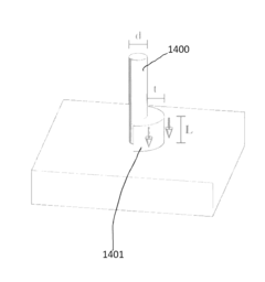
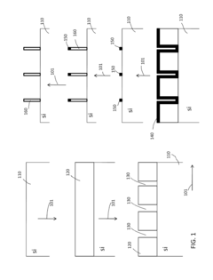
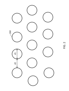
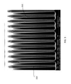
01 Fabrication methods for silicon micropillars
Various techniques are employed to create silicon micropillars, including etching processes, lithography, and deposition methods. These fabrication methods allow for precise control over the size, shape, and arrangement of the micropillars, which is crucial for their performance in different applications.- Fabrication methods for silicon micropillars: Various techniques are employed to create silicon micropillars, including etching processes, lithography, and deposition methods. These fabrication methods allow for precise control over the size, shape, and arrangement of the micropillars, which is crucial for their performance in different applications.
- Applications in solar cells and photovoltaics: Silicon micropillars are utilized in solar cell and photovoltaic technologies to enhance light absorption and improve overall efficiency. The unique structure of micropillars allows for better light trapping and increased surface area, leading to improved energy conversion rates.
- Use in microfluidic and lab-on-a-chip devices: Silicon micropillars play a significant role in microfluidic systems and lab-on-a-chip devices. They can be used for fluid manipulation, particle separation, and as support structures for various biochemical processes, enhancing the functionality and efficiency of these miniaturized systems.
- Integration with sensors and MEMS devices: Silicon micropillars are integrated into various sensors and MEMS (Micro-Electro-Mechanical Systems) devices. Their unique properties allow for enhanced sensitivity, improved signal-to-noise ratios, and increased surface area for sensing applications, making them valuable in fields such as environmental monitoring and biomedical sensing.
- Surface modification and functionalization: The surface of silicon micropillars can be modified and functionalized to enhance their properties or add new functionalities. This includes coating with various materials, chemical treatments, or attaching specific molecules to tailor the micropillars for specific applications such as catalysis, drug delivery, or selective binding.
02 Applications in solar cells and photovoltaics
Silicon micropillars are utilized in solar cell and photovoltaic technologies to enhance light absorption and improve overall efficiency. The unique structure of micropillars allows for better light trapping and increased surface area, leading to improved energy conversion rates.Expand Specific Solutions03 Use in microfluidic and lab-on-a-chip devices
Silicon micropillars play a significant role in microfluidic systems and lab-on-a-chip devices. They can be used for fluid manipulation, particle separation, and as structural elements in miniaturized analytical systems, enabling more efficient and precise biomedical and chemical analyses.Expand Specific Solutions04 Integration with sensors and MEMS devices
Silicon micropillars are incorporated into various sensors and MEMS (Micro-Electro-Mechanical Systems) devices. Their unique properties allow for enhanced sensitivity in chemical and biological sensors, as well as improved performance in mechanical sensing applications.Expand Specific Solutions05 Surface modification and functionalization
The surface of silicon micropillars can be modified and functionalized to tailor their properties for specific applications. This includes coating with various materials, chemical treatments, and the addition of functional groups to enhance their performance in areas such as catalysis, sensing, and biomedical applications.Expand Specific Solutions
Key Players in Silicon Micropillar Research and Industry
The experimental techniques for analyzing silicon micropillars are in a developing stage, with the market showing significant growth potential. The industry is transitioning from research to early commercialization, driven by increasing demand in semiconductor and microelectronics sectors. Key players like SUMCO Corp., Sony Group Corp., and SK Siltron Co., Ltd. are investing in R&D to advance these techniques. The technology's maturity varies, with established companies like Texas Instruments and Micron Technology incorporating advanced analysis methods, while newer entrants like Xi'an Yisiwei Material Technology Co., Ltd. are focusing on specialized applications. The competitive landscape is diverse, including both large semiconductor manufacturers and specialized materials research firms, indicating a dynamic and evolving market.
California Institute of Technology
Technical Solution: Caltech has pioneered several experimental techniques for analyzing silicon micropillars, with a focus on understanding their mechanical and electrical properties at the nanoscale. They have developed a novel in-situ nanoindentation technique that allows for real-time observation of deformation mechanisms in silicon micropillars using transmission electron microscopy (TEM) [14]. Caltech researchers have also employed advanced synchrotron-based X-ray microdiffraction to study the evolution of crystal structure and defects in micropillars under various loading conditions [15]. Their approach includes the use of custom-built microelectromechanical systems (MEMS) for precise control and measurement of forces applied to individual micropillars [16]. Additionally, Caltech has developed sophisticated computational models that integrate experimental data to predict the behavior of silicon micropillars under complex stress states and environmental conditions [17].
Strengths: Cutting-edge in-situ characterization techniques, access to advanced synchrotron facilities, and strong integration of experimental and computational approaches. Weaknesses: Some techniques may require specialized facilities not widely available, potentially limiting reproducibility in other labs.
Agilent Technologies, Inc.
Technical Solution: Agilent Technologies has developed a comprehensive suite of analytical instruments and techniques for studying silicon micropillars. Their approach includes high-precision atomic force microscopy (AFM) for surface topography and mechanical property measurements [9]. They have also developed specialized scanning probe microscopy (SPM) techniques for electrical characterization of individual micropillars [10]. Agilent's portfolio includes advanced mass spectrometry methods for analyzing the chemical composition and impurities in silicon micropillars with parts-per-billion sensitivity [11]. The company has integrated machine learning algorithms into their data analysis software to improve the accuracy and speed of micropillar characterization [12]. Additionally, Agilent offers customized sample preparation techniques to ensure minimal damage to delicate micropillar structures during analysis [13].
Strengths: Wide range of analytical techniques, high-precision instrumentation, and advanced data analysis capabilities. Weaknesses: Potential high cost of instrumentation and need for specialized training to operate complex equipment.
Innovative Approaches in Silicon Micropillar Analysis
Methods for fabricating high aspect ratio probes and deforming high aspect ratio nanopillars and micropillars
PatentInactiveUS20160280537A1
Innovation
- The method involves using standard photo-beam and electron-beam lithographic techniques, followed by inductively coupled plasma etching with specific etch chemistries like SF6/O2 cryogenic etch and Pseudo Bosch etch, to create high aspect ratio pillars with precise control over etch depth and sidewall angles, and subsequent metal contact formation for probes, along with deformation techniques using resist contraction to achieve controlled strain.
Methods for examination of microarrays using surface reflectance measuring tool
PatentInactiveUS20050280826A1
Innovation
- The use of a surface reflectance measuring tool that analyzes the physical characteristics of biomolecules on microarrays without altering the product, allowing for in-line inspection and detection of defects such as scratches, thumbprints, and misalignment, using a beam of controlled polarization and a collector to compile a surface reflectance map, enabling non-destructive quality control and process optimization.
Environmental Impact of Silicon Micropillar Production
The production of silicon micropillars, while offering significant technological advancements, also raises important environmental concerns. The manufacturing process involves several stages that can potentially impact the environment, necessitating a thorough assessment of its ecological footprint.
One of the primary environmental considerations is the energy consumption associated with silicon micropillar production. The fabrication process typically requires high-temperature conditions and precision equipment, leading to substantial energy usage. This energy demand often translates to increased greenhouse gas emissions, particularly if the energy source is not renewable. Efforts to mitigate this impact include the adoption of more energy-efficient manufacturing techniques and the integration of renewable energy sources in production facilities.
Water usage is another critical environmental factor. The production of silicon micropillars involves multiple cleaning and etching steps, consuming significant amounts of ultra-pure water. This not only strains local water resources but also generates wastewater containing various chemicals and particulates. Advanced water recycling systems and more efficient cleaning processes are being developed to address this issue, aiming to reduce both water consumption and wastewater generation.
Chemical usage in silicon micropillar production also poses environmental risks. Etching processes often employ hazardous chemicals such as hydrofluoric acid, which can have severe environmental consequences if not properly managed. Proper handling, storage, and disposal of these chemicals are crucial to prevent soil and water contamination. Research is ongoing to develop less harmful alternatives and to improve chemical recovery and recycling methods.
The production of silicon micropillars also generates solid waste, including silicon particles and other byproducts. While silicon itself is not typically considered toxic, the accumulation of waste materials can impact local ecosystems if not properly managed. Recycling and repurposing of silicon waste are areas of active research, aiming to create a more circular production process.
Air quality is another concern, particularly due to the potential release of particulate matter and volatile organic compounds during various stages of production. Advanced air filtration systems and emission control technologies are essential to minimize these impacts on local air quality and worker health.
Lastly, the long-term environmental impact of silicon micropillars in electronic devices must be considered. As these components become more prevalent in consumer electronics, issues of e-waste and end-of-life disposal become increasingly important. Developing effective recycling methods for devices containing silicon micropillars and designing for easier disassembly and material recovery are crucial steps in mitigating the environmental impact of this technology throughout its lifecycle.
Standardization of Silicon Micropillar Analysis Methods
The standardization of silicon micropillar analysis methods is crucial for ensuring consistency and reliability in experimental techniques for analyzing these structures. Currently, there is a lack of universally accepted protocols, leading to variations in results across different research groups and laboratories. To address this issue, a comprehensive approach to standardization is necessary.
One key aspect of standardization involves sample preparation. Establishing uniform procedures for fabricating silicon micropillars, including consistent dimensions, surface treatments, and cleaning processes, is essential. This standardization ensures that researchers worldwide are working with comparable samples, facilitating more accurate comparisons of results.
Measurement techniques also require standardization. This includes defining specific protocols for various analytical methods such as scanning electron microscopy (SEM), atomic force microscopy (AFM), and X-ray diffraction (XRD). Standardized calibration procedures, imaging parameters, and data collection methods should be established to minimize variations in measurements across different instruments and laboratories.
Data analysis and interpretation represent another critical area for standardization. Developing standardized algorithms and software tools for processing raw data from various analytical techniques can significantly reduce discrepancies in results interpretation. This includes establishing agreed-upon methods for quantifying micropillar dimensions, surface roughness, and other relevant parameters.
Reporting standards are equally important in the standardization process. Creating a standardized format for presenting experimental results, including specific details about sample preparation, measurement conditions, and data analysis methods, would greatly enhance the reproducibility and comparability of studies across the field.
Interlaboratory comparisons and round-robin tests can play a vital role in validating and refining standardized methods. These collaborative efforts can help identify potential sources of variability and lead to further improvements in standardization protocols.
Lastly, the development of reference materials and calibration standards specifically designed for silicon micropillar analysis would provide a common baseline for researchers. These standards could be used to validate measurement techniques and ensure consistency across different laboratories and instruments.
Unlock deeper insights with Patsnap Eureka Quick Research — get a full tech report to explore trends and direct your research. Try now!
Generate Your Research Report Instantly with AI Agent
Supercharge your innovation with Patsnap Eureka AI Agent Platform!